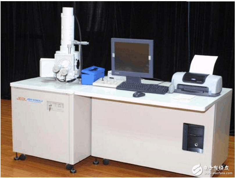
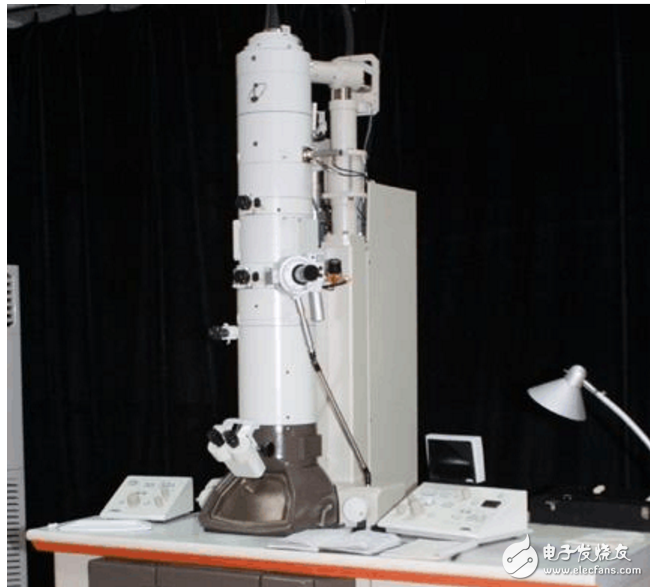
SEM, full name is scanning electron microscope, also known as scanning electron microscope, English name Scanning Electronic Microscopy. SEM: Scanning electron microscopy is a modern cell biology research tool invented in 1965. It mainly uses secondary electron signal imaging to observe the surface morphology of the sample, that is, to scan the sample with a very narrow electron beam and pass the electron beam. The interaction with the sample produces various effects, primarily secondary electron emission from the sample. The secondary electrons are capable of producing a magnified image of the surface of the sample, which is created in time series as the sample is scanned, i.e., using a point-by-point imaging method to obtain a magnified image. (1) It is possible to directly observe the structure of the sample surface, and the size of the sample can be as large as 120 mm & TImes; 80 mm & TImes; 50 mm. (2) The sample preparation process is simple and does not need to be sliced. (3) The sample can be translated and rotated in a three-dimensional space in the sample chamber, so the sample can be observed from various angles. (4) The depth of field is large and the image is full of three-dimensionality. The depth of field of a scanning electron microscope is several hundred times larger than that of an optical microscope, and several times larger than that of a transmission electron microscope. (5) The image has a wide range of magnification and a high resolution. It can be magnified ten times to several hundred thousand times, and it basically includes the magnification range from a magnifying glass, an optical microscope to a transmission electron microscope. The resolution is between the optical microscope and the TEM, up to 3 nm. (6) The damage and contamination of the sample by the electron beam is small. (7) While observing the morphology, other signals from the sample can also be used for micro-regional component analysis. 1 abnormal contrast. Due to the charging effect, the secondary electron emission is affected by irregularities, causing a part of the image to be abnormally bright and the other part to be darkened. 2 image deformity. The electron beam is irregularly deflected by the action of the electrostatic field, resulting in image distortion or phase difference. 3 image drift. Irregular displacement of the electron beam causes image drift due to the action of the electrostatic field. 4 bright spots and bright lines. Irregular discharges often occur with live samples, resulting in irregular bright spots and bright lines in the image. TEM, the full name of transmission electron microscope, also known as transmission electron microscope, English name Transmission Electron Microscope. TEM: Transmission electron microscopy, or TEM, projects an accelerated and concentrated electron beam onto a very thin sample. The electrons collide with atoms in the sample to change direction, resulting in solid angle scattering. The size of the scattering angle is related to the density and thickness of the sample, so that images with different brightness and darkness can be formed. Generally, the transmission electron microscope has a resolution of 0.1 to 0.2 nm and a magnification of tens of thousands to a million times. It is used to observe ultrastructure, that is, a structure that is less than 0.2 μm and cannot be seen under an optical microscope, and is also called “sub-displayâ€. microstructure" Portable Ev Charger,Ev Charger,Electric Car Charger,Electric Vehicle Charger Yangzhou JERI New Energy Co., Ltd. , https://www.jrevcharging.com
