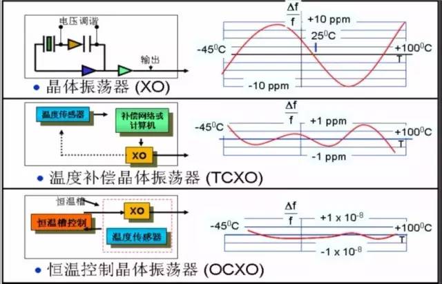
1) Constant temperature crystal oscillator (hereinafter referred to as OCXO) This type of crystal oscillator uses a constant temperature bath technology for temperature stability. The crystal is placed in a constant temperature bath. By setting a constant temperature operating point, the tank is kept at a constant temperature. The range is not affected by the external temperature, and the effect of stabilizing the output frequency is achieved. These crystal oscillators are mainly used in various types of communication equipment, including switches, SDH transmission equipment, mobile communication repeaters, GPS receivers, radio stations, digital televisions, and military equipment. This type of crystal can be equipped with a voltage control pin depending on the user's needs. The working principle of OCXO is shown in Figure 3 below: The main advantage of OCXO is that the frequency-temperature characteristics are the best among all types of crystal oscillators due to the use of the bath technology. Due to the precise circuit design, the short-term stability and phase noise are better. The main disadvantage is that the power consumption is large and the volume is large, and it takes about 5 minutes of heating time to work normally. Typical indicators of such crystals produced by our company are as follows: 2) Temperature compensated crystal oscillator (hereinafter referred to as TCXO). The TCXO temperature-compensated crystal oscillator is a quartz crystal oscillator that reduces the amount of oscillation frequency change caused by ambient temperature changes by its additional temperature compensation circuit. The principle of its temperature compensation is to compensate the frequency drift caused by the ambient temperature change of the resonator by changing the load capacitance in the oscillation circuit to change with temperature. The role of the crystal is to provide the system with a basic clock signal. Usually a system shares a crystal to keep the parts in sync. Some communication systems use different crystals for the fundamental and RF frequencies, and are synchronized by electronically adjusting the frequency. The crystal is typically used in conjunction with a phase-locked loop circuit to provide the clock frequency required by the system. If different subsystems require clock signals of different frequencies, they can be provided by different phase-locked loops connected to the same crystal. Its solution to temperature stability uses some temperature compensation methods. The main principle is to control the output frequency of the crystal oscillator by sensing the ambient temperature and appropriately transforming the temperature information to achieve a stable output frequency. The traditional TCXO is compensated by analog devices. With the development of compensation technology, many digital compensation TCXOs have begun to appear. This digitally compensated TCXO is also called DTCXO. When we use MCU for compensation, we call it MCXO. Technology, this type of crystal re-temperature characteristics achieve high precision, and can adapt to a wider range of operating temperatures, mainly used in military applications and harsh environments. With the joint efforts of the vast number of R & D personnel, our company has independently developed the high-precision MCXO, its design principle and leading in the world, coupled with a highly automated production test system, its monthly output can reach 5,000, its The design principle is shown in Figure 4. Typical application indicators for this type of crystal are as follows: 3) Ordinary crystal oscillator (SPXO). This is a simple crystal oscillator, commonly referred to as a clock, which works by removing the "voltage control", "temperature compensation" and "AGC" parts of Figure 3, completely by the free oscillation of the crystal. Such crystals are mainly used in applications where stability is not critical. 4) Voltage controlled crystal oscillator (VCXO). This is based on whether the crystal oscillator is equipped with a voltage control function. A type of crystal oscillator with a voltage-controlled input pin is called a VCXO. The above three types of crystal oscillators can all have a voltage-controlled port. The total frequency difference of the crystal oscillator: the maximum deviation of the crystal oscillator frequency from the given nominal frequency due to the combination of the specified working and non-working parameters within the specified time. Note: The total frequency difference includes the maximum frequency difference caused by the frequency temperature stability, the deviation caused by the frequency aging rate, the frequency voltage characteristics and the frequency load characteristics. Generally, it is only used in the case of short-term frequency stability, but not in other frequency stability indicators. For example: precision guided radar. Frequency stability: Any crystal oscillator, the frequency instability is absolute, the degree is different. The curve of the output frequency of a crystal with time is shown in Fig. 2. The figure shows three factors of frequency instability: aging, drift and short stability. Frequency temperature stability: The maximum allowable frequency offset without an implied reference temperature or with an implied reference temperature operating within the specified temperature range under nominal power and load. Ft=±(fmax-fmin)/(fmax+fmin) ftref =±MAX[|(fmax-fref)/fref|,|(fmin-fref)/fref|] ft: frequency temperature stability (without implied Reference temperature) ftref: frequency temperature stability (with implied reference temperature) fmax: the highest frequency measured within the specified temperature range fmin: the lowest frequency measured within the specified temperature range fref: the frequency measured by the specified reference temperature The crystal oscillator of the ftref index is more difficult to produce than the crystal oscillator using the ft index, so the crystal oscillator of the ftref index is sold at a higher price. 2500 Puffs Vpae,Mini Disposable E-Cigarette,Rechargeable Disposable Vape,Thick Oil Atomizer Vaporizer Pen Guangzhou Yunge Tianhong Electronic Technology Co., Ltd , https://www.e-cigarettesfactory.com Figure 3 block diagram of the constant temperature crystal oscillator
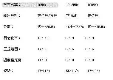
 Figure 4 MCXO digital temperature compensation crystal oscillator block diagram
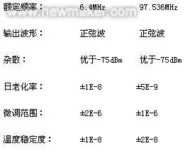
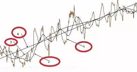 The graph 1 of the crystal oscillator output frequency changes with time. It is measured once in 0.1 second, showing the short-stabilization of the crystal oscillator; the curve 3 is measured once in 100 seconds, showing the drift of the crystal oscillator; the curve 4 is once in 1 day. The situation of the measurement. It shows the aging of the crystal.
Start-up characteristics (frequency stable warm-up time): refers to the rate of change of the frequency of a period of time (such as 5 minutes) after power-on to another period (such as 1 hour) after power-on. Indicates the speed at which the crystal reaches a steady state. This indicator is useful for frequently switched instruments such as frequency meters. Note: In most applications, crystal oscillators are powered for a long time. However, in some applications, crystal oscillators require frequent power-on and shutdown. At this time, the frequency stability warm-up time indicator needs to be taken into consideration (especially for harsh Military communication stations used in the environment, when frequency temperature stability is required to be ≤±0.3ppm (-45°C~85°C), OCXO is used as the local oscillator, the frequency stable warm-up time will be no less than 5 minutes, and only MCXO is needed. Ten seconds). Frequency Aging Rate: The relationship between oscillator frequency and time when measuring oscillator frequency under constant environmental conditions. This long-term frequency drift is caused by the slow change of the crystal component and the oscillator circuit component. Therefore, the rate of the frequency offset is called the aging rate, and the maximum rate of change after the specified time limit can be used (eg, ±10 ppb/day, power-on 72). After the hour), or the maximum total frequency change within the specified time limit (eg ±1ppm/(first year) and ±5ppm/(ten years)).
Crystal aging is due to problems such as stress, contaminants, residual gases, structural process defects, etc. in the production of crystals. The stress has to be stabilized over a period of time. A crystal cutting method called "stress compensation" (SC cutting method) gives the crystal a good characteristic. The molecules of the contaminants and residual gases are deposited on the crystal piece or oxidized by the crystal electrode. The higher the oscillation frequency, the thinner the crystal piece used, and the more the effect is. This effect will take a long time to stabilize, and this stability will be repeated as the temperature or working state changes - causing the contaminants to re-concentrate or disperse on the crystal surface. Therefore, a crystal with a low frequency is better than a crystal with a high frequency, a crystal with a long working time, a crystal with a shorter working time, and a crystal with a continuous operation than the crystal with an intermittent operation.
Note: The frequency aging rate of TCXO is: ±0.2ppm~±2ppm (first year) and ±1ppm~±5ppm (ten years) (except for special cases, TCXO rarely uses the daily frequency aging rate index because even in the experiment Under the conditions of the chamber, the frequency change caused by the temperature change will also greatly exceed the frequency aging of the temperature compensated crystal oscillator every day, so this indicator loses its practical significance). The frequency aging rate of OCXO is ±0.5 ppb to ±10 ppb/day (after 72 hours of power-on), ±30 ppb to ±2 ppm (first year), and ±0.3 ppm to ±3 ppm (ten years).
Short stability: short-term stability, the observation time is 1 millisecond, 10 milliseconds, 100 milliseconds, 1 second, 10 seconds. The output frequency of the crystal oscillator is affected by the internal circuit (Q value of the crystal, noise of the component, stability of the circuit, operating state, etc.), resulting in a wide spectrum of instability. After measuring a series of frequency values, it is calculated using the Allen equation. Phase noise can also reflect short-stable conditions (with special instrument measurements). Reproducibility: Definition: After the crystal oscillator is stable for a long time, it will be shut down after a long period of time. It will stop for a period of time t1 (such as 24 hours), boot for a period of time t2 (such as 4 hours), measure the frequency f1, then stop the same period of time t1, and then start the same For a period of time t2, the frequency f2 is measured. Reproducibility = (f2-f1) / f2. Frequency voltage control range: The minimum peak value of the crystal oscillator frequency is adjusted from the reference voltage to the specified end voltage and the crystal oscillator frequency. Description: The reference voltage is +2.5V, the specified end voltage is +0.5V and +4.5V, and the frequency-controlled crystal oscillator has a frequency change of -2ppm at +0.5V frequency control voltage, and the frequency is controlled at +4.5V frequency control voltage. The amount of change is +2.1ppm, then the VCXO voltage control frequency voltage control range is expressed as: ≥ ± 2ppm (2.5V ± 2V), the slope is positive, and the linearity is +2.4%.
Voltage Control Frequency Response Range: The relationship between the peak frequency offset and the modulation frequency when the modulation frequency changes. Usually, the specified modulation frequency is expressed by a few dB lower than the specified modulation reference frequency. Note: The frequency response of the VCXO frequency voltage control range is 0 to 10 kHz. Frequency Controlled Linearity: Output Frequency vs. Ideal (Linear) Function - A measure of the input control voltage transfer characteristic that is a percentage of the allowable nonlinearity of the entire range of frequency offsets. Note: The typical VCXO frequency voltage control linearity is: ≤±10%, ≤±20%. The simple VCXO frequency voltage control linear calculation method is (when the frequency voltage control polarity is positive): Frequency voltage control linearity = ± ((fmax - fmin) / f0) × 100% fmax: VCXO at the maximum voltage control voltage Output frequency fmin: Output frequency of VCXO at minimum voltage-controlled voltage f0: Voltage-controlled center voltage frequency Single-sideband phase noise £(f): ratio of power density to carrier power of a phase-modulated sideband from carrier f . Output waveform: From a large class, the output waveform can be divided into square wave and sine wave.
Square wave is mainly used in the clock of digital communication system. The other wave mainly has several index requirements such as output level, duty ratio, rise/fall time and driving capability. With the rapid development of science and technology, high-quality signal sources are required as carriers for increasingly complex baseband information in similar systems such as communications, radar, and high-speed data transmission. Since a carrier signal with parasitic amplitude modulation and phase modulation (unclean signal) is modulated by the baseband signal carrying the information, the spectral components (parasitic modulation in the carrier) that should not exist in these ideal states will cause the transmitted The signal quality and the data transmission error rate are obviously deteriorated. Therefore, as the carrier of the transmitted signal, the cleanness of the carrier signal (spectral purity) has a direct impact on the communication quality. For sinusoidal waves, it is often necessary to provide indicators such as harmonics, noise, and output power.