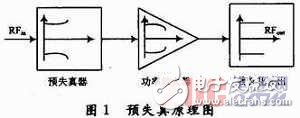
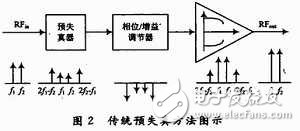
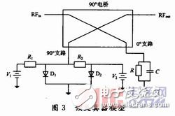
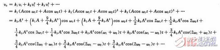
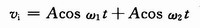
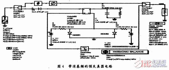
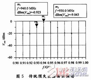
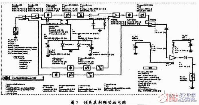
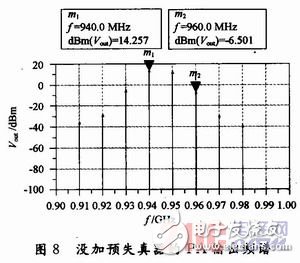
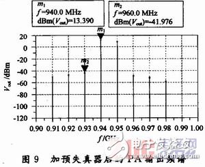
Abstract: Predistortion technology is one of the main techniques for linearization of power amplifiers. The traditional predistorter can not eliminate the characteristics of the two-tone fundamental frequency component generated at its output. A new predistorter is proposed and used to improve the nonlinear distortion of the RF power amplifier. The simulation results show that this method can significantly improve the third-order intermodulation nonlinear distortion of RF power amplifier. Key words: nonlinear distortion; RF power amplifier; cancellation fundamental frequency; predistorter; ADS The RF power amplifier is an important part of the closest transmitting antenna and is widely used in various wireless transmitting devices. The indicators of RF power amplifiers are: linearity, efficiency, noise figure, etc., the most concerned about which is its linearity and efficiency. With the increase in the number of wireless users and the development of broadband communication services, the communication frequency band becomes more and more crowded. In order to accommodate more communication channels in a limited spectrum range, a modulation technique with higher spectrum utilization rate is needed. However, due to the nonlinearity of the amplifier, the envelope fluctuation of the signal produces nonlinear distortion. This puts higher demands on the linearity of the RF power amplifier. Traditional methods for improving the nonlinear distortion of RF power amplifiers include feedforward, negative feedback, and predistortion. Feedforward linearization requires additional auxiliary power amplifiers and more complex control circuits and is bulky and expensive. The method of negative feedback technique reduces the gain of the amplifier and only allows the amplifier to operate stably in a narrow frequency band, which is only suitable for narrowband communication systems. Predistortion technology is one of the most commonly used linearization techniques. The circuit is simple in implementation, stable in operation, low in cost, wide in working frequency bandwidth, easy to integrate, and high in DC power. This article will introduce a new predistorter design and use ADS2008U1 to simulate the circuit. The results show that this scheme can improve the nonlinear distortion of the power amplifier. Predistortion is to add a nonlinear circuit at the front end of the power amplifier to compensate for the nonlinear distortion of the power amplifier. The basic principle is shown in Figure 1. The predistorter is essentially a nonlinear generator that compensates for the nonlinearity of the RF power amplifier by controlling the nonlinear generator so that its output and the nonlinearity of the RF amplifier are the same in amplitude and opposite in phase, thereby improving the power amplifier. The linearity allows the amplifier to obtain a linearized output. According to the position of the predistorter, the predistortion technology can be divided into three types: RF predistortion, IF predistortion and baseband predistortion. This paper mainly discusses RF predistortion technology. The principle block diagram of the traditional predistortion technology is shown in Figure 2. Its shortcoming is that when the input signal enters the predistorter, there is not only a nonlinear distortion signal for compensating the nonlinear characteristics of the RF power amplifier at its output, but also a residual fundamental frequency component, according to the principle of predistortion technology. It can be seen that this part of the residual fundamental frequency signal is opposite to the phase of the fundamental frequency signal in the RF power amplifier. Therefore, while improving the nonlinear characteristics of the power amplifier, its output power is also weakened to some extent. In this paper, a co-parallel diode pair predistorter is used in the form of a bridge. The predistortion model is shown in Fig. 3. 2.1 Predistorter model Using a 90° bridge network to complete the signal processing and matching functions, the capacitor on the 0° path of the bridge compensates for the reactance component of the diode pair to compensate for phase distortion. A good match of the input/output impedance characteristics can also be maintained with a 90° bridge. 2.2 Nonlinear output analysis Set the equal-tone two-tone signal vi at the input of the predistorter: Where: A is the amplitude of the two-tone signal; ω1, ω2 are the frequencies of the two-tone signal. Let the nonlinear distortion coefficient of the predistorter be y=f(x), and the output be v0, that is, v0=f(vi). Spread it into a power series form: It can be seen from the above equation that in the output signal of the predistorter, there are not only the fundamental frequency signal but also the harmonics and various intermodulation signals. Among them, the third-order intermodulation distortion component is needed, and the fundamental frequency component generated here can be called “interference signal†for the design, and the circuit must be designed to eliminate the fundamental frequency signal. 2.3 Design of a new predistorter For the problem that the predistorter output has a fundamental frequency signal that is not needed by the system, a new type of predistorter is designed to eliminate the fundamental frequency signal. The circuit schematic is shown in Fig. 4. The input equal-amplitude two-tone signal is divided into two by the 3 dB splitter, one signal enters the predistorter, and the other signal is delayed by the delay and enters the gain/phase adjuster. The delay is primarily to synchronize the signal entering the gain/phase adjuster with the signal entering the predistorter. Wherein, the gain/phase adjuster is formed by cascading the adjustable attenuator and the adjustable phase shifter, and the function thereof is to obtain a fundamental frequency signal with appropriate amplitude and phase. In addition, the output of the predistorter will contain a series of nonlinear distortion components, including the fundamental frequency, which, after appropriate delay, are sent to the power combiner along with the output signal of the gain/phase regulator. By controlling the attenuation of the attenuator and the phase of the phase shifter, a signal having the same amplitude and opposite phase as the fundamental frequency signal included in the predistorter output signal is generated to cancel the fundamental frequency component produced by the predistorter. The signal obtained at the output of the power divider is the required third-order intermodulation distortion signal. 2.4 Predistorter simulation analysis The circuit simulation model was built in Agilent's ADS2008U1. The simulation circuit adds equal-amplitude two-tone signals as shown in Figure 4. The frequencies are 940 MHz and 950 MHz, respectively. Perform harmonic balance (HB) simulation analysis on the circuit to obtain the spectrum of the predistorter output signal as shown in Figure 5 and Figure 6. Figure 5 shows the simulation results of the conventional predistorter, and Fig. 6 shows the simulation results after adding the cancellation frequency circuit. By comparison, it can be seen that after adding the cancellation frequency circuit, the fundamental frequency component of the signal at the output of the predistorter is reduced by 40 dBc. 3.1 Design indicators and construction of pre-distortion power amplifier circuits Performance indicators of the predistorter RF power amplifier: operating frequency range is 900 MHz to 1 GHz; output power is greater than or equal to 13.4 dBm; third-order intermodulation improvement is greater than or equal to 40.2 dBc. The simulation uses a packaged power amplifier module, which contains the power tube MRF9742 and the DC bias circuit and the input/output matching circuit. The predistortion power amplifier circuit is shown in Figure 7. 3.2 RF power amplifier simulation results The simulation results are shown in Figure 8 and Figure 9. Figure 8 shows the output spectrum of the power amplifier without the predistorter. Figure 9 shows the output spectrum of the power amplifier with the predistorter added. This paper designs a predistorter with a cancellation frequency and uses this predistorter to improve the nonlinear distortion of the RF power amplifier. The simulation results show that the predistorter designed by this paper can significantly compensate the shortcomings of the traditional predistorter, and can suppress the third-order intermodulation distortion component of the RF power amplifier by more than 40 dBc. The improvement of this paper is that the adaptive method can be used to control the adjustable phase shifter and attenuator in the circuit, and the attenuator and phase shifter can be adaptively adjusted by detecting the proportion of the third-order intermodulation distortion component in the output signal. This can better improve the nonlinear distortion of the rate amplifier. AAWG WDM - Athermal Arrayed Waveguide Gratings Wavelength Division Multiplex
There are currently three types of DWDM technologies developed in the industry, which are based on AWG, TFF and FBG technologies. AWG is a planar waveguide device, which is an arrayed waveguide grating made on a chip substrate using PLC technology. Compared with FBG and TTF, AWG has the advantages of high integration, large number of channels, low insertion loss, and easy mass automated production.
The Athermal AWG module is based on the arrayed waveguide grating technology and does not require additional power supply or temperature control. It is a pure passive module. It has the characteristics of low loss and polarization-related loss, low crosstalk, etc., and has good stability in the operating temperature range of -40°C to 85°C.
With the vigorous development of 5G, users will have higher and higher requirements for bandwidth. Operators will need to continuously increase data transmission rates, increase transmission capacity, and reduce operating costs. Among them, the active WDM-PON solution is difficult to deploy on a large scale due to its high cost; while the passive WDM-PON will have more application space due to its advantages of low cost, no power supply, and easy installation. Among them, the non-thermal AWG will be more widely used because of its larger number of channels, denser channel spacing, and no need to rely on power supply or temperature control.
Athermal AWG WDM, also known as Athermal Arrayed Waveguide Grating WDM and AAWG WDM Splitter, along with FBT WDM splitter, LAN WDM splitter, Filter WDM splitter, dense WDM splitter and coarse WDM splitter, are the most commonly used WDM device in construction of PON.
Athermal AWG WDM, Athermal Arrayed Waveguide Grating WDM, AAWG WDM Splitter Shenzhen GL-COM Technology CO.,LTD. , https://www.szglcom.com