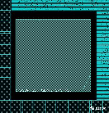
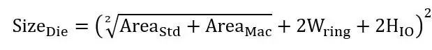
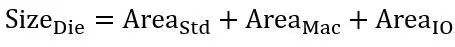
The concept of chip area estimation The main covered area of ​​the chip area is divided into three parts IO: signal and power pad of the chip Standard cell : Implementing the functional logic of the chip Macro block: Third-party IP (PLLDAC POR Memory .etc) The chip area estimation is the process of counting the total area of ​​the main part through the library information of the target process, the design spec, the information of the previous design, and the partial IP report. Figure 1, IO, Standard cell, Macro block The specific process of chip area estimation Get area information Obtain IO area: Obtain the length, width, and size of various IOs through the IO library file of the target process, and then count out the pad selection and quantity in the spec, pin_list document according to our design. Obtain the area of ​​Standard cell: statistics can be collected through the synthesis of individual IPs. The conversion project section is based on the original full-chip synthesis report. For IPs that do not have a complete RTL, the designer can provide estimates based on the complexity of the IP. The number of logic gates is calculated by the number of equivalent logic gates*. ※Equivalent logic gate: The complexity of digital design is generally evaluated by the number of equivalent logic gates. The equivalent logic gate is generally a standard size (minimum drive capability) of the target process, and the NAND gate represents A (10k Gates). ) B(um2)=C(mm2), SMIC 110nm B=4.12. Get Macro block area: The IP document provided by the third-party IP provider will have the shape and area, and the memory document generated by Memorycompiler will also have the shape and area of ​​the memory. Several area estimation methods With the above three kinds of area basic information, area estimation can be performed. First of all, the area information of the obtained standard cell and Marco block should be converted, and the standard cell conversion (if the total area of ​​the Standard cell is SCAN but SCAN is not inserted, it needs to multiply by the area increment after SCAN, and the empirical value 105%) Mainly due to the density ◎, the total area of ​​the Standard cell needs to be divided by the density value. The Macro block is mainly due to the blockage. ◠The length of the Macro block plus twice the width of the blockage must be multiplied. ◠density: Due to the Timing of the chip, etc., the area for placing the Standard cell cannot be completely filled by the Standard cell (the blue part in FIG. 2 ), and the total area of ​​the Standard cell is the percentage of the area for placing the Standard cell. It is density. Figure 2 Standard cell, idle area (including power wiring) ◠blockage: third-party IP (mostly analog IP, central blue square in Figure 3) In order to prevent electrical interference in the external environment, in the document will require the reservation of a certain empty area or surrounded by a power ring, this part is the blockage. image 3 Pad Limit In this case, the entire IO of the chip is tightly packed on all four sides. The area in the middle is larger than the sum of the converted Standard cell and Macro block. Because there is no way to shrink the IO on the four sides, the main area of ​​the chip is determined by the IO arrangement. The area of ​​this area does not need to be estimated by back-end engineers arranged directly IO directly given 2. Core Limit In this case, all the IOs of the chip are tightly packed on the four sides, and the area in the middle is smaller than the area of ​​the CORE (the sum of the converted Standard cell and Macro block). At this time, the area of ​​the CORE determines the size of the chip area. Core Limit's design was based on the fact that the IO ring could not be placed on other units, and the CORE was evaluated as a square (since the area was wasted on the wafer during the chip production, and it was advantageous to have internal power supply wiring on the chip. IRdrop), square the square of the area value to square plus the width of a ring (power ring, etc.) with a fixed width or percentage of side length, plus twice the height of IO, and then square Get the main area of ​​the chip. If Core Limit design does not require the placement of other units on the IO ring, the estimate is to add the CORE area to the IO area. When the chip is produced, many chips on a wafer need to be separated by a dicing machine. At this time, the space reserved for dividing the chip is scribe line. During chip separation and chip transportation and packaging, the chip is The edge of the stress will change, the design needs to do a circle in the perimeter of the chip (sealring) to protect the chip is not broken and shielded and moisture-proof function. Thus, the area of ​​the entire chip is the width of the chip body side (square area of ​​the main body) plus twice the width of the scribe line and twice the square of the sealring width.
Sports can't be abandoned more freely
Professional sound engineering technology
Bluetooth In Ear Headset,Wireless In Ear Headset,In Ear Headset Wireless,Headset Wireless In Ear Guangzhou HangDeng Tech Co. Ltd , http://www.hangdengtech.com


Close ergonomic design, close to the ear, even wearing for a long time can also enjoy comfortable experience.
And can form a triangular stable support with the ear, even if running and riding, vigorous fitness is still close to the ears, wildly shake off.
customized stainless steel acoustic structure, high quality grahene hoop system and obvious environmental noise attenuation will open up a pleasant journmey journey for you to enjoy the sound.
Built-in microphone/ Effective noise reduction/ Clear call/ Easy to carry