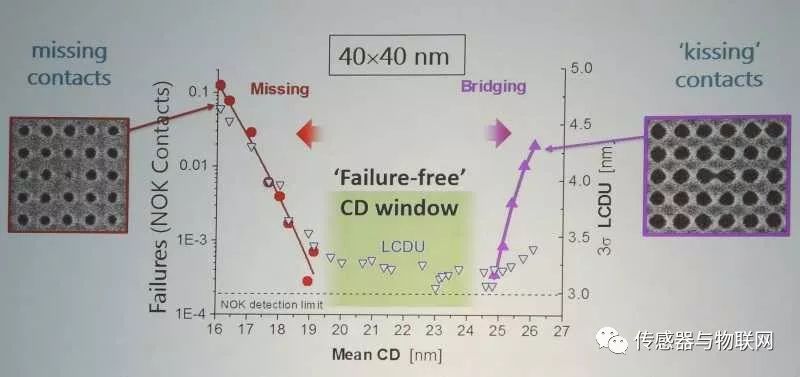
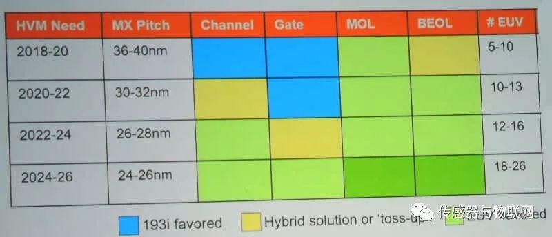
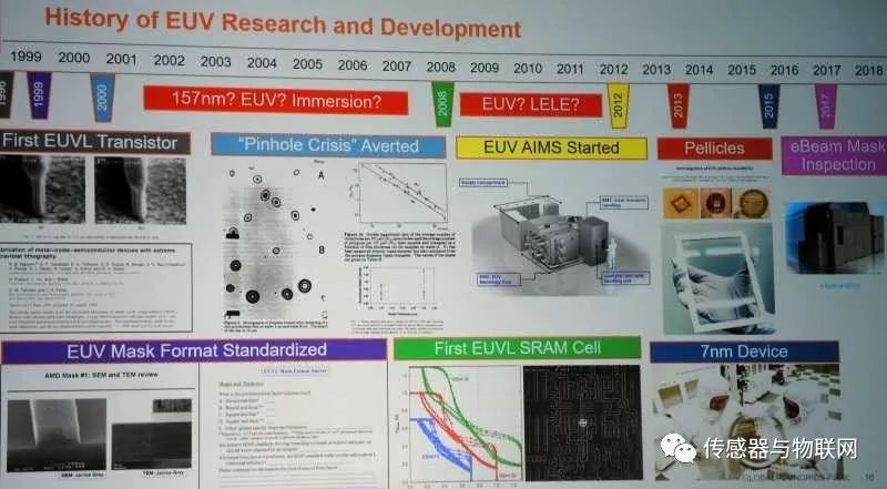
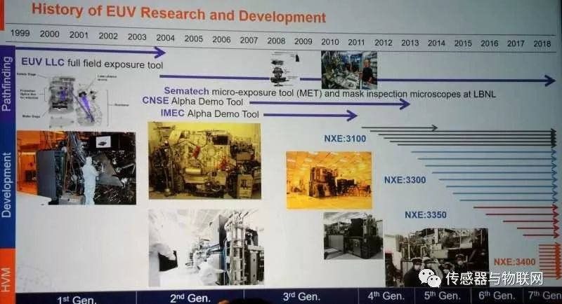
Extreme ultraviolet photolithography (EUV) technology is said to exhibit random defects at the 5 nanometer (nm) node. According to researchers, currently they are adopting a series of technologies to eliminate these defects. However, so far, no effective solution has been found. The news came as Globalfoundries, Samsung and TSMC competed to upgrade their EUV system to a highly available 250W light source for next year's 7nm production. Today, the emergence of these random defects shows that there is no panacea for solving the problem of the increasing cost and complexity of semiconductor manufacturing. Greg McIntyre, a graphic expert at the Imec Research Institute in Belgium, said at the SPIE Advanced Lithography Conference held in California, USA that the latest EUV scanner can print the 20nm planned by the foundry for 7nm. And the larger size of the key specifications. However, their ability to make fine lines and holes is not yet clear. Optimists like McIntyre believe that a series of solutions will soon emerge for this so-called "random effect." However, some skeptics believe that such an outcome is just one more reason to question the EUV system. Is an expensive and long-delayed EUV system really a mainstream tool for chip manufacturers? Former Intel lithography expert Yan Borodovsky expects that industry engineers should be able to use the EUV stepper for 2-3 exposures to create 5nm or even 3nm components. However, in his keynote speech at the event, he also pointed out that as chip defects continue to rise, engineers will eventually be forced to adopt new fault-tolerant processor architectures such as neural networks. The most recent defect suddenly appeared at a critical size of around 15nm, which is the technological node required to manufacture a 5nm chip for the manufacturing process in the 2020s. EUV manufacturer ASML mentioned in last year's event that the company is preparing a next-generation EUV system that can print finer geometries, but these systems will not be available until after 2024. Imec researchers pointed out that EUV lithography will appear random defects at 5nm (Source: Imec) Random defects come in many forms. Some are caused by imperfect holes; others are linear cracks, or short circuits between two wires and two holes. Because of the tiny size of these defects, researchers sometimes spend several days to find them. McIntyre describes the challenges that will be encountered when discovering and eliminating errors. For example, some researchers have proposed a standard method of measuring line roughness, which is one of the keys to understanding defects. Another problem is that it is not yet clear what happens when the photoresist material hits the EUV light source. McIntyre pointed out, "We don't know yet how many electrons are produced and what chemical substances will be created... We are not completely aware of physics, so we are conducting more experiments." He pointed out that researchers have tested up to 350 Combination of photoresist and process steps. Good yield at 7nm/5nm “Manufacturing will be severely hit by lower yields... If I'm responsible for this, then I would say it's time to retire,†said a retired lithography technologist at a seminar on the 5nm defect. . Technologists from Globalfoundries made more optimistic but relatively sensible views in another keynote speech. George Gomba, vice president of globalfoundries research, said during his review of EUV's 30 years of commitment to EUV: “This is a difficult task and there is still more work to do.†Today's NXE 3400 system "does not meet some of our expectations of the roadmap requirements, so there is still some uncertainty (at 7nm). If you do not increase productivity and availability, we may find it difficult to maximize the value of EUV." Gomba pointed out that random defects at 5nm include subtle 3D fractures and tears, such as gaps in lines. He also called for more work on so-called actinic systems so that lithography technicians can detect EUV masks before covering them with masks. "In order to fully utilize EUV, we will need a photochemical detection system. Although it is still under development, it can be used to assist e-beam mask detection systems that are currently available." Globalfoundries shares its views on when and how to import EUV. (Dark green box indicates high numerical aperture EUV is more popular (Source: Globalfoundries) In an interview, Borodovsky stated that another factor that may cause 5nm defects is the lack of uniformity of existing EUV photoresist materials. In addition, he also expressed support for direct electron beam writing because the complex phase shift mask used by EUV will eventually expand to 8 times the price of current immersion masks. Multibeam, a company founded by Lam Research founder David Lam, recently received $35 million in government funding for its electron beam technology. He hopes to create a commercial system that can be applied to the market in two and a half years, but the version suitable for mass production will take longer. Imec believes that the next generation of EUV is expected to be commercialized by 2025 Borodovsky said that by 2024, defects may become so common that traditional processors will not be manufactured with advanced technology. Experiments using memory arrays and built-in embedded operands may be more fault-tolerant, such as IBM's True North chip, and HP Labs' efforts to create memristors. Globalfoundries Review EUV Development History Globalfoundries Spokesperson Outlines Major Milestones for EUV R&D in the Past 30 Years 10 Mm Nano Tip,Smart Board Touch Screen Pen,Electronic White Board Pen,Infrared Touch Screen Pen Shenzhen Ruidian Technology CO., Ltd , https://www.wisonens.com