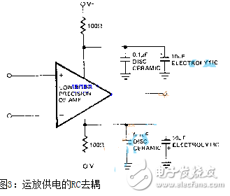
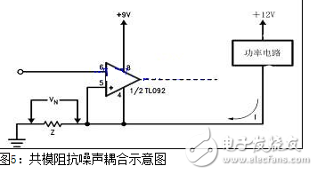
Power ripple In the circuit of the full-wave rectified linear regulated power supply, the 100Hz ripple is the main power supply noise. For the op amp circuit, the 100Hz noise level usually requires to be controlled within 10nV-100nV (RTI), which depends on three factors: The power supply rejection ratio (PSRR) at 100 Hz, the ripple rejection ratio of the regulator and the size of the input filter capacitor of the regulator. Figure 1 is the PSRR-frequency curve of OP77. It can be seen that the PSRR of OP77 is about 76dB at 100Hz. To obtain a performance of no more than 100nV (RTI), the ripple of the power supply must be less than 0.6mV. Commonly used three-terminal voltage regulators generally provide about 60dB of ripple suppression. In this case, the input filter capacitor of the regulator must be large enough to limit the input ripple to less than 0.6V. Power supply decoupling Typical power supplies powered by series regulators contain noise with an amplitude of 150uV and a frequency range of 100Hz-100KHz. The switching power supply is more serious. The PSRR of the op amp is reduced at a frequency of 20dB / Decade at high frequency. Adding RC or LC decoupling network to the foot can filter out most of the noise. The circuit form is shown in Figure 3. When using RC decoupling, it should be noted that changes in load current will cause modulation of the voltage on the power supply pin. Power regulation Any change in the power supply voltage will cause a change in the input bias current of the op amp. The PSRR of the OP77 in Figure 1 is 126dB (0.5uV / V) at DC. The change in the power supply voltage is a potential source of low-frequency noise. In the application of low-noise op amps, it is important to reduce the ripple of the power supply and increase the regulation rate of the power supply. Inadequate power regulation rate usually causes unpleasant low-frequency noise. Switching power supply The switching power supply is a very serious noise source. The following figure is the voltage waveform at the output of a typical switching power supply: It can be seen that the noise spectrum contains both the switching frequency and its harmonic components, as well as the high-frequency components of the damped oscillation caused by the resonance of the switching circuit, which extends from tens of KHz to tens of MHz, while the ordinary op amp is placed at hundreds of Hz Above, PSRR starts to drop sharply, and it is almost zero at several hundred KHz. At this time, the power supply noise appearing at the output terminal will be very serious. Channels and countermeasures In addition to paying attention to the selection of PSRR or CMRR parameters of the op amp and strengthening the decoupling of the op amp power supply (such as the use of RC decoupling), in the design of the switching power supply, the following aspects should be noted: Noise in the power supply may be directly coupled to the input of the amplifier through leakage from the reference source or PCB. Pay attention to the filtering of the voltage reference source output. For PCB leakage, you can add a ground wire protection between the signal input lead and the power trace. Noise may be directly coupled to the amplifier input through distributed capacitance between PCB traces, causing interference. When wiring the PCB, pay attention that the power line and the weak signal line should not be close to the parallel wiring, the net distance of the line is greater than 3 times the line width (3W principle), and add ground between the power line or digital signal line and the analog small signal line Line isolation. Improper ground handling, noise affects sensitive circuit parts through common impedance. In order to prevent the common impedance from introducing power supply noise into the signal loop, pay attention to the following points: avoid large current with noise flowing through the previous small signal ground on the ground; single-point grounding, separate grounding of the power supply, analog and digital circuits; layout ground The plane layer minimizes the impedance of the ground wire; the output of the switching power supply is drawn from the ground terminal of the last filter capacitor to avoid the output from the ground terminal of the capacitor in front of the filter inductor. The displacement current driven by the switching voltage of the drain of the switch tube passes through the primary and secondary distributed capacitance, the secondary circuit, the secondary to the earth and the stray capacitance, the stray capacitance between the earth and the primary ground forms a loop, and the secondary analog circuit flows through The common-mode current flowing through the unbalanced impedance is converted into a differential mode, causing interference to the amplifier circuit (see Figure 6). The interference introduced by the common mode is generally the high-frequency component of the switching noise (more than a few MHz). The measures mainly include the following three points: providing a low-impedance noise bypass channel from the secondary ground of the switching power supply to the primary ground, usually using a safety capacitor of 1000p ~ 2200p; using a common mode choke to enhance the common mode of the output of the switching power supply Filtering; Use isolation techniques to minimize common-mode current in the loop. It is coupled to a signal loop or a ground loop with a certain loop area through a spatial magnetic field, causing an impact on the signal. In addition, high-frequency interference from the switching power supply or the mains network may be directly coupled to the signal loop through the space stray capacitance. Design considerations include: reasonable layout, adjustment of inductor coil or transformer placement direction, optimized wiring, reducing the loop area of ​​key signals, and avoiding formation of ground loops to reduce interference; double-sided or single-panel wiring, pay attention to signal lines and Ground wire, power wire and ground wire must be close to parallel wiring; use 1000p capacitor RF multi-point grounding, which can take into account the requirements of EMC and low-frequency signal-to-noise ratio; add shielding to sensitive circuits, pay attention to the reference of the shielding layer to the protected signal Ground; in the design of the wiring, pay attention not to tie the power cable and the signal cable together. summary The main measures to reduce power supply noise in the design of op amp circuits include: Through decoupling, filtering and other measures to reduce the ripple and noise components of the power output. Improve the design and increase the power supply voltage regulation rate. Reasonable circuit structure, elaborate PCB wiring, and reasonable routing technology. Select devices with higher PSRR or CMRR in the sensitive noise band.
Germany type 16A 250V~, IP20, Class I, non-rewirable, single-way socket outlet complies ,with shutter, with a non-rewirable plug, with cord H05VV-F 3G1,0-1,5mm 2 (max length be 2m for 1,0mm 2 and 30m for 1,5mm2 ).
16A 250V~, IP20, Class II, non-rewirable, with single way socket-outlet with shutter, with a non-rewirable plug, with flexible cord H05VV-F (with or without fabric braided cover) 2G1,0-1,5mm 2 (Max. 2m for 1,0mm 2 in length and Max.30m for 1,5mm 2 ). Germany Extension Cord,Power Strip Extension Cord,European Extension,Eu European Power Extension Cord CIXI KYFEN ELECTRONICS CO.,LTD, , https://www.kyfengroup.com