The design of electronic circuit is a very complicated system engineering. In the design process, the designer analyzes the specific data, and then proposes the preliminary design plan, and then carries out corresponding modification and debugging, and continuously designs the circuit. Complement and improve the circuit design. This process is very complicated and time consuming. With the advent of electronic design automation (EDA) technology, the time for designing electronic circuit courses has been greatly saved, making the design of electronic circuits more accurate, accurate and scientific. 1 Characteristics of EDA technology At present, EDA technology has been widely used in electronic circuit design, printed circuit board design, programmable device programming, and integrated circuit board design. By using EDA technology, the corresponding designers can automatically design all aspects of circuit design, logic analysis, timing testing, performance design and so on. For the development of EDA software technology, Multisiim8.0 software support platform is a powerful support platform to play the role of EDA technology, which can ensure the processing and analysis process of its circuit establishment, experimental data analysis and structure output. Completed in the integrated system. In the process of designing with EDA technology, designers only need to perform simple operations with the mouse to complete the circuit creation, change circuit parameters, replace circuit components and so on. At the same time, in the process of using EDA technology for circuit design, the soft can perform the test of the corresponding design scheme, continuously analyze the performance of the design circuit, and repair and modify the loopholes and problems in the circuit design. To optimize the circuit performance of the design. At the same time, the application of EDA technology in the Multisiim8.0 software support platform for circuit design and optimization, the software has no hard requirements in the input and output instructions and various control languages, and does not need to correspond to the various aspects of the circuit. The programming requires only the virtual electronic components to be connected by nodes and lines in the circuit design platform, and the corresponding simulation waveforms and analysis results of various parameters can be obtained from the virtual instrument table. The Multisiim 8.0 software platform has a large number of virtual models corresponding to the actual components, which makes the circuit design form closer to the reality in the corresponding electronic circuit design, making the simulation effect more Precise and scientific. Figure 1 Basic process 2.2 Develop corresponding design plans Figure 2 sequential circuit design Article Source: Electronic Products World Disclaimer: This article is a reprinted article. The purpose of reprinting this article is to pass on more information. The copyright belongs to the original author. If it involves infringement, please contact Xiaobian for processing. The Moser Electronics Design Circle is developed and operated by Mouser Electronics to serve the global electronics design community. The company distributes more than 600 leading brands and can order more than 4 million online products for design engineers and procurement personnel. Provide one-stop shopping platform, welcome to follow us and get first-hand design and industry information Guangdong Kaihua Electric Appliance Co., Ltd. , https://www.kaihuacable.com
Electronic Design Automation (EDA) technology is a modern electronic technology designed by using computers as a platform for work, through the integration of electronic technology, intelligent technology and computer technology. With the continuous deepening of modern education, the application of EDA technology is becoming more and more extensive.
2 General steps for electronic circuit design using EDA technology
2.1 Understand the corresponding design topics
Before designing an electronic circuit, it is necessary to conduct a full-scale analysis of the circuit to be designed, and to master the functional requirements, design standards, design components, and technical specifications of the design circuit, and to characterize the processed signal and the controlled conversion object. The parameters are analyzed and statistically analyzed. The basic process of its design is shown below: 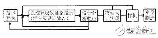
By analyzing the overall function of the system, the schematic block diagram of the circuit design is drawn, and then the overall design is divided into multiple links. Through the analysis of the links between different links, the way of signal communication between each link and the timing of circuit operation are determined. The overall block diagram of the circuit design should be able to simply and clearly express the process and principle of the entire circuit design.
2.3 Simulation experiment on unit circuit
After determining the overall design plan, the components should be selected, the circuit diagram of each link should be drawn by electronic simulation software, and then the simulation function in the electronic simulation software should be used to simulate the test to judge the design of the link. Whether the plan is feasible. If COMS, discrete components, TTL, op amp integrated circuits and other components are used in the design of the circuit, and different power supplies are used, then the level shifting process between circuits should be carried out during the design process. Design, and draw the corresponding block diagram of the way and process of conversion to ensure that its level is converted correctly. At the same time, when designing the simulation circuit, you can select the appropriate simulation software according to the type of circuit to be designed. At present, many kinds of simulation software with different emphasis have been developed in the power industry, including SPICE, Proteus, Multisim and other software. In general, for the simulation process of the basic circuit in circuit design, the best choice is to use Multisim software for simulation experiments; for relatively complex control circuits, it mainly uses Proteus software; in communication engineering In the circuit design, when designing the simulation experiment, MATLAB software is generally used. Through the use of various simulation circuit software, it is possible to perform corresponding performance verification on the design of each link, simulate the principle and process of its operation, and automatically analyze the parameters in the circuit design scheme. The deficiencies are improved to optimize the design. Through the use of EDA technology, not only can the design process be simple and convenient, it saves a lot of time, and it can develop the innovative thinking of the corresponding learners and improve their hands-on ability.
2.4 Analysis of the design scheme between the links
After using the EDA technology to simulate the unit circuit, the feasibility of the whole circuit should be analyzed. Because in the simulation experiment of each unit, the performance of some of them is tested, which makes even if there is no problem in each link, but when combined into a whole, there may be unreasonable matching between the links. The situation, so that the performance of the entire system does not meet the expected goals. Therefore, after conducting simulation experiments on each link, it is necessary to conduct a comprehensive analysis of the circuits of each link, and carry out in-depth analysis on the signal input and output relationship, the polarity of each link interface, and the timing of each link. Conflicts and contradictions in circuit design, and then modify them to develop the best design.
2.5 Combining design links
After verifying the design scheme between each link circuit and each link circuit, the entire design plan should be simulated to verify the feasibility of the whole design. After designing the corresponding circuit components according to the design requirements, it is necessary to carry out repeated experiments and connections, so that the designers can master the design of the circuit. At the same time, due to the ideal components and ideal connection process in the electronic simulation experiment, there are many factors affecting the performance stability of the actual circuit. Therefore, in the physical installation of the circuit, its performance should be debugged multiple times to achieve the best performance.
3 case analysis
3.1 Design of combinational logic circuit
Through the general steps of electronic circuit design, the design steps of the combinational logic circuit can be introduced: analyzing the problem, listing, evaluating the expression, and drawing the circuit diagram. Below we will discuss the logic simulation design of whether the circuit of two input signals is the same.
3.1.1 Setting rules. Set the two input signals to A and B respectively, and set the output signal to X. When the input circuits of the two signals A and B are the same, output X=0. When the input circuits of the two models A and B are different, the output is different. Is X=1.
3.1.2 Start the electronic work platform (EWB), enter its main interface, open the instrument database of the platform, search for the logic converter, double-click its icon to open the operation panel of the logic converter, the true value on the panel In the table area, click the two logical variables A and B respectively, so as to establish a two-variable truth table in the output area of ​​the panel, and input the corresponding logical value in the output variable column according to the corresponding requirements.
3.1.3 After entering the corresponding input quantity in the logic converter, click the “truth table → simplify logical expression†option on its panel, so that the simplified logical expression is displayed in the logic expression bar at the bottom of the panel. .
3.1.4 After the simplified logical expression is displayed at the bottom of the logic converter panel, select the “Expression → Non-Logical Circuit†option on the panel, and then display the five NAND gates in the corresponding display area. Circuit.
3.1.5 After the circuit is designed, its logic function should be tested by connecting two switches at two inputs, one of which selects “+5V†and the other selects ground, and its output is connected to the indicator light. Connect, then turn on the switch and verify the status in the truth table according to the status of the indicator.
3.2 sequential circuit design
A frequency divider is designed, which is mainly composed of JK flip-flops.
3.2.1 First, test the logic function of the JK trigger. Select a JK flip-flop from the corresponding digital device library, request the trigger itself to be low-level trigger, set and reset, connect according to the following figure, close the simulation switch in the circuit, and then open the logic analyzer panel. By reading the above graphics and parameters, and analyzing them, you can complete the test of the logic function of the JK trigger. 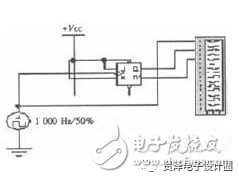
3.2.2 By using the characteristics of the JK flip-flop, the trigger is assembled as required to have a corresponding crossover function. In general, a JK flip-flop can be made into a two-divider, and the corresponding combination of the two dividers can be assembled into a four-divider. According to the design requirements, it is concluded that the eight-divider needs to be used in the circuit design. Then, three flip-flops need to be connected according to the binary step-counter stage connection to obtain the eight-divider. After the frequency divider is assembled, the pulse of the clock and the Q terminal of the JK flip-flop are connected to the logic analyzer, and the corresponding waveform diagram can be obtained. The output terminal can be obtained by the waveform diagram. The relationship between the high and low levels and the time pulse.
4 Understanding the role of EDA technology and its prospect analysis
At present, the application of EDA technology is more and more common, and the role played in the field of electronic circuit design is becoming more and more important, which requires us to correctly understand the role of EDA technology. In my opinion, the education and guidance for the correct application of EDA technology mainly comes from educators, which requires relevant educators to face up to EDA technology, rationally and fully utilize teaching resources, and actively adopt new methods and new modes of education and teaching. Ways to explore ways to accelerate modern education. At the same time, in the corresponding education and teaching process, EDA technology should be introduced into the formal teaching curriculum, combined with the corresponding experiments, thus effectively accelerating students' understanding of this technology. However, in the process of education and teaching, we must adhere to the principle of seeking truth from facts, we must not exaggerate its functions, or rely on this kind of technology to ban traditional manual experiments, leading to students' practical ability and ability to think. Development is limited.
In my opinion, EDA technology is now in a stage of rapid development, and with the continuous development of various large-scale FPGA devices, the hardware standards of EDA technology in its simulation and design have been greatly developed. . In the next few years, EDA technology will continue to develop toward large-scale integrated circuits, and its hardware and software IP core will be further confirmed in related application fields, and its SOC efficient and low-cost design will continue to mature. .
5 Conclusion
By applying EDA technology to the design and simulation process of electronic circuits, the learning mode is changed to novelty and interest. It can fully mobilize the enthusiasm of students to learn and exert students' subjective initiative, thus effectively improving students' circuits. The ability to design and analyze. At the same time, through the combination of traditional teaching methods and simulation technology, the application of virtual technology to the actual design process has improved the requirements for the corresponding educators and accelerated the progress of the curriculum reform. It is a powerful force to promote the process of socialist modernization. means.