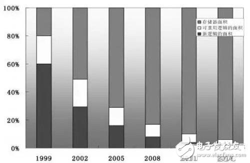
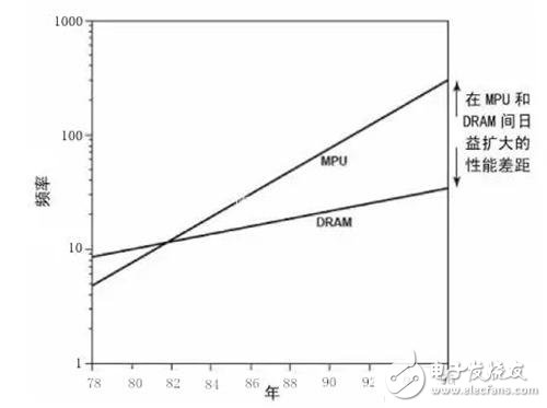
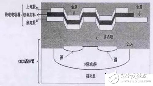
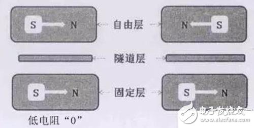
With the development of VLSI technology, humans have entered the ultra-deep sub-micron era. Advanced processes enable people to integrate processors, memory, analog circuits, interface logic, and even RF circuits onto a large-scale chip to form a so-called SoC (system on a chip). Embedded memory, which is an important part of SoC, will gradually increase its proportion (area) in SoC. Let's take a look at the related content with Xiaobian. Recently, TSMC’s technical director Sun Yuancheng unveiled eMRAM (embedded magnetoresistive random access memory) and eRRAM (embedded resistive memory), which were developed for the first time in the platform of their own technology, to be risky in the next year. Trial production. It is expected that the trial production will mainly use the 22nm process. This next-generation storage will provide faster and lower power storage for the four areas of the Internet of Things, mobile devices, high-speed computing computers and smart cars. This move by TSMC allows embedded memory to return to people's attention again. This article will explain the past and present of embedded memory for you. Embedded memory is no longer a new concept. Compared with the off-chip memory, the embedded memory refers to the memory integrated in the chip and the IP, mixed signal and other IP in the system to form a single chip. Now it has become a basic component of the SOC chip, and almost every embedded memory in each SOC chip has a certain proportion. According to whether the data will be lost after power failure, the embedded memory can be divided into two categories, one is volatile memory and the other is non-volatile memory. Volatile memory refers to data loss after power failure, mainly including fast speed, low power consumption SRAM and high density DRAM. Non-volatile memory is just the opposite. In practice, it mainly includes eFlash, EEPROM, and next-generation memories such as eMRAM, eRRAM, and ePRAM. Although they are all memories, they are still slightly different. The most important difference between embedded memory and discrete memory is that embedded memory is often related to the process characteristics of the application IC itself, such as chips made with 90nm and 45nm processes, and the internal embedded memory size. The difference is also great. Discrete memory devices are optimized primarily around memory device processes. With the development of information technology, the proportion of embedded memory in the SOC is also increasing year by year. As can be seen from Figure 1, it has increased from an average of 20% in 1999 to 60-70% in 2007 and even in 2014. 90% of the area. It can be seen that the impact of embedded memory on the performance of the chip system is increasing. Figure 1 The proportion of embedded memory in the SOC's chip area Back in the 1960s and 1970s, the semiconductor industry was dominated by IDM, and each company did its own work from chip design, manufacturing to packaging. Each family independently develops its own processes, IP and related chips. In the early days, the requirements of the system, including integration, speed, and power consumption were not high. Therefore, discrete memory occupied the mainstream position at that time and became the first choice of various application manufacturers. Later, in the 1980s and 1990s, the fabless and foundry models began to emerge. Based on the complexity of the design and the product design cycle, third-party independent IP vendors such as ARM began to emerge. As chip integration continues to increase, it in turn presents two major challenges to discrete memory: 1) integration and process start to allow more memory to be integrated on-chip; 2) memory speed development lags far behind MPU speed The MPU speed is growing at 60% per year, while the memory is only 10%. The difference between the speeds of the two is shown in Figure 2. Figure 2 Diagram of the development of MPU in DRAM over time At the same time, the on-chip memory has a flexible and simple interface, lower latency and wider bus, and more importantly, it can save the space of the system, making it increasingly popular among integrated circuit designers. Embedded memory is mainly presented in both SRAM and DRAM formats during this period. By the mid-1990s, Intel made a major innovation that integrated off-chip caches into chips. This directly led to the collapse of a large number of discrete off-chip cache vendors at the time, becoming a landmark event for embedded memory instead of discrete memory. Today, more than 90% of a mobile phone processor is composed of various embedded SRAMs such as register files, one-level cache or even three-level cache. Embedded SRAM has also become a process technology measurement index for foundries. Since SRAM consists of six transistors, and DRAM consists of only one transistor plus one capacitor, which has an area advantage, many manufacturers were thinking about the possibility of embedding DRAM into the system. In the 1990s, large companies such as IBM and Toshiba were trying to develop embedded DRAM. However, the development is not smooth. The difficulty in development is that the DRAM process is quite different from the conventional logic process, and the integration of the process is quite difficult. Although today, with the advancement of technology, some companies like TSMC are re-examining the feasibility of eDRAM, and some results, but the mainstream design has not included eDRAM into the necessary options. Later, with the rapid growth of consumer electronics, the ever-expanding storage demand has spurred the development of embedded flash (eFlash). From an early stage, designers simply fixed the program in ROM, to later OTP, EEPROM and even high-density eFlash memory that is now hot. Embedded memory can store code and data efficiently, and it is not lost after power-off, which is of great significance for many applications. However, today, some of the defects exposed by existing storage technologies, such as SRAM and DRAM, are its volatility. After the power is cut off, information will be lost and susceptible to electromagnetic radiation. This defect greatly limits its defense aviation. A series of key high-tech applications such as aerospace. The writing speed of FLASH and EEPROM is slow, and the writing algorithm is complex, which can not meet the requirements of high-speed and high-reliability writing in real-time processing systems, and the power consumption is high, which can not meet the low power requirements of embedded applications. There is a higher demand for the performance of existing information storage products, and there is an urgent need to make breakthroughs in storage materials and technology. Driven by these demands, new nonvolatile memories such as ferroelectric memory (FRAM), phase change memory (PRAM), magnetic memory (MRAM), and resistive memory (RRAM) have emerged. Although these are new types of memories, from a certain perspective, these memories have existed for some time. The ferroelectric memory is a non-volatile memory that does not lose information after power-off, and has the advantages of high speed, high density, low power consumption, and radiation resistance. Its core foundation is ferroelectric crystal material, which uses ferroelectric effect as its charge storage mechanism, and has the characteristics of random access memory (RAM) and non-volatile storage products. Its structure is shown below. The working principle of FRAM is to use a metal-ferroelectric-semiconductor field effect transistor structure. The ferroelectric film is used to replace the gate silicon oxide layer in the MOS tube. The ferroelectric film maintains two stable polarization states, respectively, indicating "1" "and "0"". Figure 3 FRAM structure sectional view MRAM is made using the principle that the magnetic field of a material changes with the action of a magnetic field. The tunneling magnetoresistance effect of the magnetic memory cell magnetic tunnel junction (MTJ) is used for storage. As shown in Figure 4 below, the MTJ has three layers, the uppermost layer is the free layer, the middle is the tunnel junction, and the bottom is the fixed layer. The direction of polarization of the magnetic field of the free layer can be changed, while the direction of the magnetic field of the fixed layer is fixed. When the free layer is parallel to the magnetic field of the fixed layer, the memory cell exhibits a low resistance state; when the magnetic field direction is opposite, the memory cell assumes a high resistance state. The MRAM determines whether the stored data is 0 or 1 by detecting the level of the memory cell resistance. Figure 4 Schematic diagram of MJT structure
We produce Lighting for commerical ,industrial ,and household . Specially for desk lamp LED which 360 degree bent freely .It can brighten you in any angle as
you want. Road light and functional light also.
Home Outdoor Lighting LED Stadium Light LED Floodlight LED Tri-proof Light LED Street Light LED Garden Light LED Canopy Light Indoor Lighting LED Panel Light LED Batten Light GL Series LED Batten Light GLK Series LED Batten Light
Home Lighting & Furnishings - Quality, Style and Selection. Lamps Plus offers a complete selection of indoor and outdoor lighting fixtures. From stylish ceiling light fixtures, chandeliers and trend-setting ceiling fans to thousands of designer lamps and lamp shades that are in-stock and ready to ship.
Home Light,Led Desk Lamp,Rgb Night Lamp,Bathroom Lights Jiangmen soundrace electronics and technology co.,ltd. , https://www.soundracegroup.com