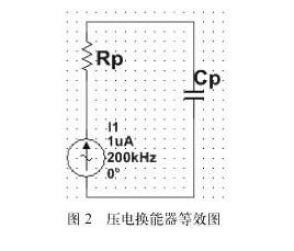
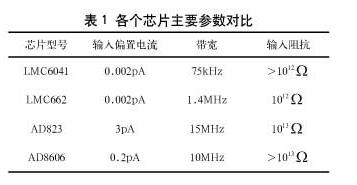
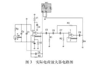
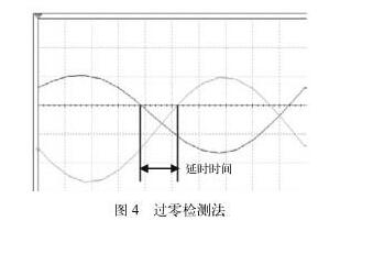
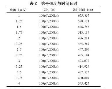
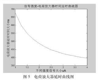
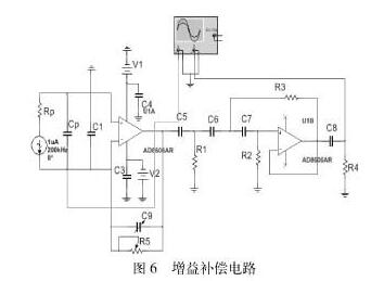
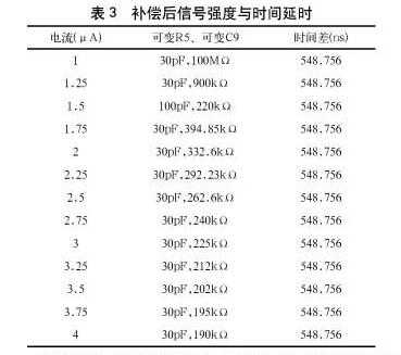
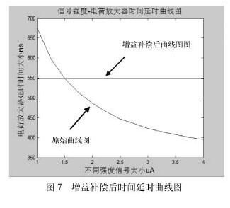
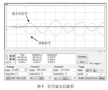
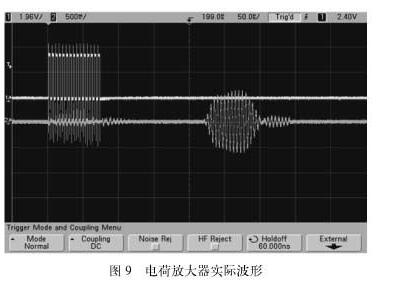
A charge amplifier is an essential signal conditioner when testing a system with a voltage transducer. It is an op amp that directly converts a small amount of charge into a low-impedance voltage signal, so it is often used as a transducer conversion circuit. For a gas ultrasonic flowmeter, any test session will affect the accuracy of the measurement. Therefore, it is necessary to use Multisim12 to simulate the charge amplifier. During the simulation, it is found that the delay of the charge amplifier is changing under different signal intensities, which has a serious impact on the measurement accuracy. Therefore, it is necessary to adopt a gain compensation measure in the charge amplifier circuit, and design a gain compensation circuit so that the delay of each measurement is equal, which can greatly improve the measurement accuracy of the ultrasonic gas flow meter. At the same time, the circuit simulation software is used to compensate the gain circuit. Simulations were performed to verify the rationality of parameter selection. A piezoelectric transducer is a transducer made of a positive and negative piezoelectric effect of a piezoelectric material. As the name suggests, a transducer refers to a device 12 that can perform energy conversion. The equivalent circuit of a piezoelectric transducer is related to its vibration mode, which is the equivalent of Mason's equivalent circuit. The equivalent circuit of the piezoelectric sensor is shown in Figure 1 near the resonant frequency. In Figure 1, CO is the transducer shunt capacitor, and C1, L1, and R1 represent the transducer series capacitor, series inductor, and series resistor, respectively. In the equivalent circuit, the series resonant frequency of the transducer is fs, and the series inductance LI and the reactance of the series capacitor CI cancel each other out, and the impedance of the transducer is Z==R1. At the series resonant frequency, the transducer is equivalent to one emitter. While the parallel resonant frequency is f, the impedance of the transducer reaches a maximum, at which point the transducer is equivalent to a receiver. In the charge amplifier of this paper, the piezoelectric transducer is equivalent to a receiver. The voltage of the voltage transducer measured by the bridge is f; 200 kHz, and the voltage is 1 V, the measured R, = 1.441 k8, C; 2.107 nF. Since the charge amplifier does not have a direct charge source signal, considering that the piezoelectric transducer is output as a current, the sensor can be considered as a current source. The magnitude of the current value is calculated based on the sensitivity and sound pressure value of the receiving circuit. Its piezoelectric transducer simplifies the equivalent circuit as shown in Figure 2. The internal structure of the ultrasonic sensor is a piezoelectric crystal. When the pressure sensor is stressed, it generates a very small amount of charge, which brings certain difficulties to the rear circuit. Therefore, we need to design a new type of charge amplifier. The signal is first input to a very high input impedance, very low bias current and wide bandwidth charge amplifier. Only under the condition of very high input impedance, the input end of the charge amplifier has almost no shunt, so the operation current All flow into the feedback loop, so that the leakage of the charge can be reduced to within the range we require. According to the selection requirements of the integrated op amp described above, I chose the main parameters of the LMC662, AD823, LMC6041 and AD8606 chips. Contrast (as shown in Table 1), and related simulations, after comprehensive comparison and verification, the AD8606 chip was selected as the chip of the charge amplifier. Figure 3 is a schematic diagram of the actual charge amplifier simulation circuit designed in this paper. In the figure, the charge amplifier can only be incompletely compensated internally, and it is bound to generate self-oscillation. In the operational amplifier, a compensation circuit composed of capacitor C1 can be connected to eliminate self-oscillation. The new charge amplifier circuit can be regarded as a capacitive negative feedback gain integrating amplifier, so the charge amplifier feedback capacitor C9 must be selected in the same way as the feedback capacitor of the integral network. The new charge amplifier output sensitivity is adjusted by adjusting the charge amplifier's feedback capacitor C9. To achieve. It is required that the value of the feedback capacitor C9 cannot be too small, otherwise the distributed capacitance will have a great influence; but the value of the feedback capacitor C9 cannot be too large, otherwise the leakage is too large. The charge amplifier uses capacitive negative feedback, so the charge amplifier is equivalent to open-loop for the DC operating point, resulting in a large zero drift. To reduce the zero drift and stabilize the charge amplifier, an integral drift leakage resistor is generally connected in parallel across the feedback capacitor. R5 (10" or more) provides feedback and provides DC feedback to keep the charge amplifier circuit operating. In this paper, the Multisiml2 simulation software is used to simulate the charge amplifier circuit. The simulation circuit has two main purposes: first, pay attention to the delay variation of the charge amplifier under different signal strengths. Second, it is required to simultaneously detect the effect of the signal being amplified by the charge amplifier. Because the accuracy of the time measurement determines the measurement accuracy of the propagation time of the ultrasonic gas flowmeter, it is required to see the phase difference of the signal at different current intensities. The phase difference measurement method generally has a threshold method, a peak-to-peak measurement method, and a zero-crossing detection method. The threshold method first assumes a value. When the signal passes this value, it is used as the basis for measurement. However, the current and voltage values ​​under different signal strengths are constantly changing. We cannot use the threshold method to measure the small signal phase difference. The peak-to-peak measurement measures the maximum positive or negative value of two waveforms. However, when the small signal is measured with the peak-to-peak value, the noise will have a great influence on the peak-to-peak detection. Although this measurement method is simple, the accuracy is not very high. The zero-crossing detection method is a classical modulation domain analysis method. By measuring the time difference between two zero-crossing signals of the same frequency, the time delay of the charge amplifier is determined, as shown in FIG. This method is simple, reliable, and practical, enabling high-precision measurements. This paper takes the second wave zero-crossing as the benchmark to measure the time delay. The time delay is measured at different signal strengths with Multisim12 emulated charge amplifiers, as shown in Table 2. According to the data in Table 1, the signal strength and time delay curves written in MATLAB are shown in Figure 5. As shown in Figure 5, the delay time of the charge amplifier will decay exponentially with the signal strength, so the delay caused by the charge amplifier changes greatly, which has a serious impact on the experimental measurement results. In order to overcome this drawback, it is necessary to design a gain compensation circuit to improve the accuracy of measuring the propagation time of the ultrasonic gas flow meter. The time gain compensation circuit we designed is shown in Figure 6. The gain compensation is mainly achieved by using a sliding slip varistor and a charge amplifier. The piezoelectric sensor transmits the ultrasonic signal with continuity, and adjusts the resistance of the sliding varistor according to the strength of each received ultrasonic signal, so that the delay of the charge amplifier is maintained at a fixed value. This ensures that the delay of each detection signal passing through the charge amplifier is the same, improving the accuracy of the measurement. Therefore, as long as you choose a reasonable core, the difference between the people and the people, and the size of the feedback resistor, so that the front west line does not fall and the back curve rises, the purpose of gain compensation can be achieved, so that it can be very good. The time delay caused by the compensation of the charge amplifier. In Figure 6, the magnitude of the current at different signal strengths is ensured by the delay of the charge amplifier by adjusting the variable capacitance and the variable resistance. as shown in Table 3. It can be seen from Fig. 7 that the time delays are equal regardless of the strength of the signal through the charge amplifier after the gain is compensated by the gain. This makes the measurement time more accurate. The waveform of the signal after passing through the charge amplifier and filter circuit at 200 kHz and 1 uA is shown in Figure 8. From Figure 8, we can see that the signal amplified by the charge amplifier works well. The original signal has a voltage of about 300 uV, and the amplified signal is about 20 mV. The practical application effect provides a reliable theoretical basis for the practical application. The charge amplifier has a good effect in practical application. Figure 9 shows the actual waveform obtained by the oscilloscope after the signal is amplified. It can be seen from Fig. 9 that the clutter interference is basically within 200mV. The signal to noise ratio is very high. Since the simulation provides a reliable theoretical basis for practical applications, the charge amplifier is very effective in practical applications. Figure 9 shows the actual waveform obtained by the oscilloscope after the signal is amplified. It can be seen from Fig. 9 that the clutter interference is basically within 200mV, and the signal-to-noise ratio is Very high. The charge amplifier designed in this paper is for the amplification of small signals such as ultrasonic flowmeters. The time delay of the signal changes when passing through the charge amplifier. Therefore, gain compensation is an important part of the charge amplifier circuit. This paper presents a compensation gain circuit design scheme, which shows that it has a good gain compensation effect.
BIOTEPT Single Phase Resilient Base Motors, resilient (cradle) mounted, capacitor start-type, ball bearing motors for fan and blower service. Moderate starting torque electrical design to reduce stress on fan blades during start-up. Capacitor-type design has higher energy efficiency rating than split phase, single phase fan and blower motors. Suitable for belt-driven fans or fan-on-shaft applications. Self-ventilated design, may be mounted outside of the fan`s airflow.
Single Phase Resilient Base Motors for use where water and dust exposure is minimal. Ideally suited for use on pumps, compressors, blowers, fans, and belted applications.
Include:
DRIP-PROOF ODP • SINGLE PHASE RESILIENT BASE
TEFC • SINGLE PHASE RESILIENT BASE
PREMIUM EFFICIENCY FAN MOTORS
Resilient Base Motor,Single Phase Resilient Base Motors,Plit Phase Resilient Base Motor,Odp Resilient Base Motor Ningbo Biote Mechanical Electrical Co.,Ltd , https://www.biotept.com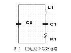
DRIP-PROOF • SINGLE PHASE
RESILIENT BASE


