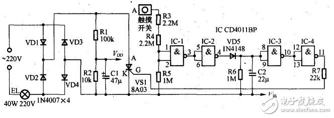
Speaking of the touch delay switch, I believe everyone is very strange, but Xiaobian wants to tell you that the touch delay switch is actually the light of the corridor in daily life, and some of the voice control is to touch, and Xiaobian today is to say the touch delay. When the switch is turned on and inform everyone to touch the delay switch wiring, please see the introduction of the touch delay switch wiring below. Touch delay switch wiring diagram The delay switch has a touch delay switch, an acousto-optic control delay switch, and the like. Just touch the touchpad of the switch by hand or give it a sound signal to automatically illuminate. When the person automatically turns off within 30 seconds to 75 seconds, the product is highly recommended by the Ministry of Energy. The touch delay switch uses the same principle as the test pencil, that is, a large resistor is connected in series between the human body and the power source, so that a low voltage current is formed through the human body (the voltage is low, but the current is not necessarily small) Finally, it flows into the earth to form a trigger circuit. In this way, the delay switch can be triggered to start timing, and the main circuit of the lamp is turned on, and the light is turned on. In the switching circuit, the acoustic detection uses the electret microphone MIC, and the triode T2 constitutes the amplifier. T2 is in a saturated conduction state when there is no sound, and when there is a sound, the microphone MIC receives an acoustic signal, which can turn off T2. The brightness detection is done by the photoresistor RG. The circuit uses a CMOS digital integrated circuit CD4011 that contains four 2-input NAND gates. One of the CD4011 is used directly as a two-input NAND gate as the discriminating circuit, and the other three are connected as inverters for the amplifier. D6, R6, C4 form a delay circuit. The switch uses a thyristor T1. The diodes D1~D4 and the thyristor T1 form a controllable rectifying circuit. When T1 is turned on, the bulb LAMP is illuminated; when T1 is turned off, the bulb is extinguished. The touch delay switch has a metal sensing chip on the outside, and a human touch generates a signal to trigger the triode to conduct, charging a capacitor, and the capacitor forms a voltage to maintain a FET conduction lamp to illuminate. When the handle is removed, the charging of the capacitor is stopped. After a period of time, the capacitor is discharged, the gate of the FET becomes a low potential, enters the cut-off state, and the bulb is extinguished. The touch delay switch circuit is on the right side of the dotted line is the ordinary lighting circuit, and the left part is the electronic switch part. VD1~VD4 and VS form the main circuit of the switch, and the IC constitutes the switch control circuit. Normally, VS is in the off state and the light is off. VD1~VD4 output 220V pulsating DC current through R5 current limit, VD5 voltage regulation, C2 filter output about 12V DC power for IC use. At this time, the LED lights up, indicating the position of the switch, which is convenient for finding the switch at night. The IC is a dual-D flip-flop, and only one of the D flip-flops is used to connect it to a monostable circuit. In steady state, the 1 pin outputs a low level, and the VS turns off. When the human hand touches the electrode M, the human body leakage current is divided by R1 and R2, and the positive half circuit turns the monostable circuit, the 1 pin outputs the high level, and the R4 is applied to the gate of the VS to turn on the VS. bright. At this time, the output of the 1 pin is high, and the capacitor C1 is charged through R3, so that the level of the 4 pin is gradually increased until the transient ends, the circuit is turned back to the steady state, the 1 pin is abruptly changed to the low level, the VS loses the trigger voltage, and the alternating current crosses zero. The time is turned off and the light is turned off. The above is the introduction of the touch delay switch wiring. Many times there are many things in life. We don't know how to use it for layout. Therefore, Xiaobian wants to take this opportunity to introduce the touch delay switch wiring and let you need it in the future. It is easy to carry out the touch delay switch wiring and finally achieve high quality results. The figure shows the experimental circuit of the touch delay switch. It consists of a full-wave bridge rectifier circuit composed of rectifier diodes VD1~VD4, which is used as an integrated circuit working power supply, and a four-input NAND gate 4011 and a unidirectional thyristor VS1 form a touch switch circuit. The full-wave bridge rectifier circuit outputs up to 200V pulsating DC power, which is divided by resistors R1 and R2, and filtered by capacitor C1 to output about 13V DC power as IC working power. When the illumination lamp EL is bright, the total current of the 4011 steady-state operation is less than 20μA, and the current of the 401l (with the 50μA range) when the lamp is off is almost impossible to measure, which shows the low power consumption of the CMOS integrated circuit. In addition, when the illumination lamp EL is lit, the R2 partial pressure drops to 2V, and the 4011 can still work, which is why the CMOS digital integrated circuit is selected. When the metal piece A end is touched by hand, the inductive alternating current signal is applied to the input terminal of the IC-1 through the step-down resistors R3 and R4. When the alternating current is in the positive half cycle, the pins 1 and 2 of the IC-1 are at a high level. The output terminal drops to a low level, and the IC-2 output terminal 4 is raised to a high level, and the timing capacitor C2 is charged through the switching diode VD5, so that the IC-3 input terminal rises to a high level, and its output terminal The 10 pin is low level, the IC-4 output terminal 11 is high level, and is applied to the unidirectional thyristor control electrode G through the resistor R7, triggering the VS1 to be turned on, and the load illumination lamp EL is lit. When the C2 charge is gradually discharged through the timing resistor R6, causing the voltage to drop below the CMOS gate turn-on voltage, the IC-3 output rises to a high level, the IC-4 output is low, and the unidirectional thyristor blocks. , EL goes out. When R6 is 1MΩ and C2 is 10μF, the touch switch control delay is about 17s, when C2 is changed to 22μF, the delay is doubled, and C2 is 47μF delay is more than enough. In the touch switch circuit, R5 is a pull-down resistor. Although its resistance value is 1MΩ, the input voltage of the NAND gate IC-1 is low, indicating that the input impedance of the CMOS digital integrated circuit is very high. The remaining input terminals of the four-input NAND gate 4011 cannot be left floating, and the parallel connection mode is used as the non-door. The IC can also use four 2-input or non-gate 4001.
3"~5" speaker (76~128mm)
1)3" speaker 78mm speaker
FAQ
Q1. What is the MOQ? 3" Speaker 78Mm Speaker,3.5" Speaker 89Mm Speaker,3.6" Speaker 91Mm Speaker,4" Speaker 102Mm Speaker Shenzhen Xuanda Electronics Co., Ltd. , https://www.xdecspeaker.com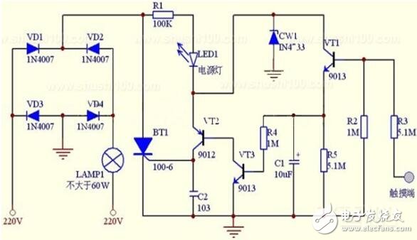
2)3.5" speaker 89mm speaker
3)3.6" speaker 91mm speaker
4)4" speaker 102mm speaker
5)5" speaker 128mm speaker


XDEC: 2000pcs for one model.
Q2. What is the delivery lead time?
XDEC: 15 days for normal orders, 10 days for urgent orders.
Q3. What are the payment methods?
XDEC: T/T, PayPal, Western Union, Money Gram.
Q4. Can you offer samples for testing?
XDEC: Yes, we offer free samples.
Q5. How soon can you send samples?
XDEC: We can send samples in 3-5 days.