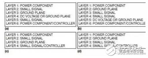
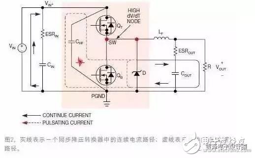
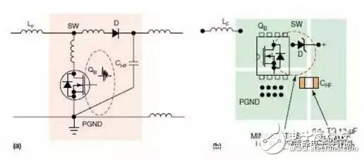
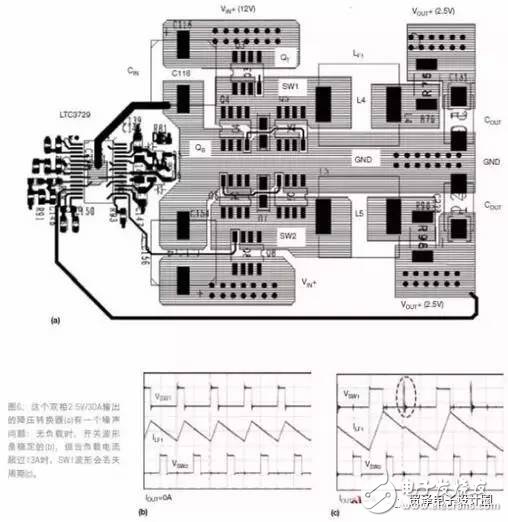
A good layout design optimizes efficiency, slows thermal stress and minimizes the effects of noise between traces and components. All of this stems from the designer's understanding of the conduction path and signal in the electrical flow. When a prototype power board is used for the first time, the best case is that it not only works, but also quiet and low heat. However, this is rare. A common problem with switching power supplies is the "unstable" switching waveform. In some cases, jitter in the segment magnetic component produces audible noise. If the problem is on the layout of the printed circuit board, it may be difficult to find the cause. Therefore, the correct PCB layout at the beginning of the switching power supply design is critical. A good layout design optimizes power efficiency, slows thermal stress, and more importantly, it minimizes noise and the interaction between traces and components. To achieve these goals, designers must understand the current conduction path and signal flow inside the switching power supply. For the correct layout design of non-isolated switching power supplies, this article gives some lessons. For an embedded dc/dc power supply on a large board, for optimum voltage regulation, load transient response, and system efficiency, the power supply output is placed close to the load device, minimizing interconnect impedance and conduction on the PCB traces. Pressure drop. Ensure that there is good air flow and limit thermal stress; if forced air cooling is used, place the power supply close to the fan position. In addition, large passive components (such as inductors and electrolytic capacitors) must not block airflow through low surface packaged semiconductor components such as power MOSFETs or PWM controllers. In order to prevent switching noise from interfering with the analog signal in the system, it should be avoided to place sensitive signal lines under the power supply as much as possible; otherwise, an internal ground plane should be placed between the power supply layer and the small signal layer for shielding. The key is to plan the location of the power supply and the need for board space during the early design and planning phases of the system. Sometimes designers ignore this advice and focus on the more "important" or "exciting" circuits on large system boards. Power management is seen as an afterthought, and the power is placed on the extra space on the board. This is a disadvantage for efficient and reliable power supply design. For multilayer boards, a good method is to place a DC or DC input/output voltage layer between the high current power component layer and the sensitive small signal trace layer. The formation or DC voltage layer provides an AC ground for shielding small signal traces from high noise power traces and power components. As a general rule, the ground plane or DC voltage layer of a multilayer PCB should not be separated. If this separation is unavoidable, the number and length of traces on these layers should be minimized, and the routing should be kept in the same direction as the large current to minimize the effects. The a and c in the figure below are the poor layer structure of the six-layer and four-layer switching power supply PCBs, respectively. These structures sandwich the small signal layer between the high current power layer and the ground plane, thus increasing the capacitive noise coupled between the large current/voltage power layer and the analog small signal layer. Figure 1 Layout structure of the switching power supply PCB The b and d in the above figure are good structures for the six-layer and four-layer PCB designs, respectively, to help minimize interlayer coupling noise, and the ground plane is used to shield small signal layers. The main point is: Be sure to place a ground plane next to the outer power level layer. Use a thick copper foil for the external high-current power layer to minimize PCB conduction loss and thermal resistance. The switching power supply circuit can be divided into two parts: a power stage circuit and a small signal control circuit. The power stage circuit contains components for transmitting large currents. In general, these components are first placed and then small signal control circuits are placed at specific points in the layout. The high current trace should be short and wide to minimize PCB inductance, resistance and voltage drop. This is especially important for traces with high di/dt pulse currents. The following figure shows the continuous current path and pulse current path in a synchronous buck converter, the solid line represents the continuous current path and the dashed line represents the pulse (switch) current path. The pulse current path includes traces connected to the following components: an input decoupling ceramic capacitor CHF; an upper control FET QT; and a lower synchronous FET QB, and an optional parallel Schottky diode. Figure 3a shows the PCB parasitic inductance in a high di/dt current path. Due to the parasitic inductance, the pulsed current path not only radiates the magnetic field, but also produces large voltage ringing and spikes on the PCB traces and MOSFETs. In order to minimize the PCB inductance, the pulse current loop (so-called thermal circuit) should have a minimum circumference when it is laid, and its trace should be short and wide. The high frequency decoupling capacitor CHF should be a 0.1μF~10μF, X5R or X7R dielectric ceramic capacitor with very low ESL (effective series inductance) and ESR (equivalent series resistance). Larger capacitive dielectrics (such as Y5V) may cause large drops in capacitance values ​​at different voltages and temperatures, and are therefore not the best material for CHF. Figure 3b provides a layout example for the critical pulse current loop in a buck converter. In order to limit the voltage drop and the number of vias, the power components are placed on the same side of the board, and the power traces are also placed on the same layer. When you need to move a power line to another layer, select a trace in the continuous current path. When using vias to connect PCB layers in high current loops, use multiple vias to minimize impedance. Figure 4 shows the continuous current loop and pulse current loop in the boost converter. At this time, the high frequency ceramic capacitor CHF should be placed near the output of the MOSFET QB and the boost diode D. Figure 5 is a layout example of a pulse current loop in a boost converter. At this time, the key is to minimize the loop formed by the switching transistor QB, the rectifier diode D, and the high-frequency output capacitor CHF. Figure 5 Pulse current loop layout in the boost converter Figure 5 shows the thermal loop and parasitic PCB inductance in the boost converter (a); the recommended layout (b) to reduce the thermal loop area. Figure 6 provides an example of a synchronous buck circuit that emphasizes the importance of decoupling capacitors. Figure 6a is a two-phase 12VIN, 2.5VOUT/30A (max) synchronous buck power supply using the LTC3729 dual-phase single VOUT controller IC. At no load, the switching node SW1 and SW2 waveforms and output inductor current They are all stable (Figure 6b). However, if the load current exceeds 13A, the waveform of the SW1 node begins to lose its period. When the load current is higher, the problem is worse (Figure 6c). Figure 6 synchronous buck circuit This problem can be solved by adding two 1μF high-frequency ceramic capacitors to the input of each channel. The capacitors isolate and minimize the thermal loop area of ​​each channel. Even at maximum load currents up to 30A, the switching waveform is stable. In Figures 2 and 4, the SW voltage swing between VIN (or VOUT) and ground has a high dv/dt rate. This node has a rich high-frequency noise component and is a powerful source of EMI noise. To minimize the coupling capacitance between the switch junction and other noise-sensitive traces, you may make the SW copper area as small as possible. However, in order to conduct large inductor currents and provide a heat sink for the power MOSFET, the PCB area of ​​the SW junction cannot be too small. It is generally recommended to place a grounded copper foil area under the switch junction to provide additional shielding. If there is no heat sink in the design for surface mount power MOSFETs and inductors, the copper foil area must have sufficient heat sink area. For DC voltage junctions (such as input/output voltage and power ground), a reasonable approach is to make the copper foil area as large as possible. Multiple vias help to further reduce thermal stress. To determine the appropriate copper area of ​​a high dv/dt switch junction, a design balance must be made between minimizing dv/dt related noise and providing good MOSFET heat dissipation. Keep the control circuit away from the high-noise switch copper foil area. For a buck converter, a good way is to place the control circuit close to the VOUT+ terminal, and for the boost converter, the control circuit is close to the VIN+ terminal, allowing the power trace to carry continuous current. If space permits, there is a small distance (0.5" to 1" between the control IC and the power MOSFET and inductor (which are both high noise and high heat components). If space is tight and you are forced to place the controller close to the power MOSFET and inductor, pay special attention to the ground or ground traces to isolate the control circuitry from the power components. The control circuit should have an independent signal (analog) ground different from the power level. If there are separate SGND (signal ground) and PGND (power ground) pins on the controller IC, they should be routed separately. For control ICs with integrated MOSFET drivers, the small signal portion of the IC pin should use SGND. Only one connection point is required between the signal ground and the power ground. A reasonable approach is to return the signal ground to a clean point in the power formation. Two types of ground can be realized by connecting only two grounding traces under the controller IC. This pad should be soldered to the PCB to minimize electrical impedance and thermal resistance. Multiple vias should be placed in the ground pad area. Two or more adjacent conductors can create a capacitive coupling. The high dv/dt on one conductor couples current through the parasitic capacitance on the other conductor. To reduce the coupling noise of the power stage to the control circuit, the high noise switching traces should be kept away from sensitive small signal traces. If possible, place the high-noise traces and sensitive traces on separate layers and use the internal ground plane as a noise shield. Space allows the control IC to have a small distance (0.5" to 1" from the power MOSFET and inductor, which is both noisy and hot. The specific controller pins, current levels and noise sensitivity are unique, so specific trace widths must be selected for different signals. Typically, small signal networks can be narrower, with traces from 10mil to 15mil wide. The high current network (gate drive, VCC, and PGND) should be wider, and the specific width is defined by the current.
In modern clinical medicine, ventilator, as an effective means to artificially replace the function of spontaneous ventilation, has been widely used in respiratory failure caused by various reasons, anesthesia and respiratory management during major surgery, respiratory support treatment and emergency resuscitation. It occupies a very important position in the field of modern medicine. A ventilator is a vital medical device that can prevent and treat respiratory failure, reduce complications, and save and prolong patients' lives.
With excellent quality and preferential prices, Kable-X (Su Zhou) Technology Co., Ltd. provides services for the wiring harness industry in various fields such as industrial control, medical care, automobiles, and new energy. It has obtained IATF16949\ISO9001\ISO14000\UL\ISO13485\IPC620, etc. Industry certification. At the same time, the company also passed the certification of high-tech enterprises in 2019 and obtained a number of industry patents. It has the ability to integrate wiring harnesses and electronic components and hardware injection molding parts. It actively participates in customers' initial product design selection, and Maintain the greatest flexibility to meet the various needs of customers. Punctual delivery to meet customer needs. Suzhou Kable-X Wire Harness Processing Factory adheres to the business philosophy of "Integrity, Responsibility, Innovation", and perfect after-sales service to create together with customers. A better tomorrow!"
We produce a large number of Medical Cable Assembly, including Ventilator Wire Harness, Medical Defibrillator Wire Harness and Medical Aid Equipment Wire Harness.
Ventilator Wire Harness,Wire Harness Manufacturing,Wiring Harness Price,Electronic Wiring Harness Assembly Kable-X Technology (Suzhou) Co., Ltd , https://www.kable-x-tech.com