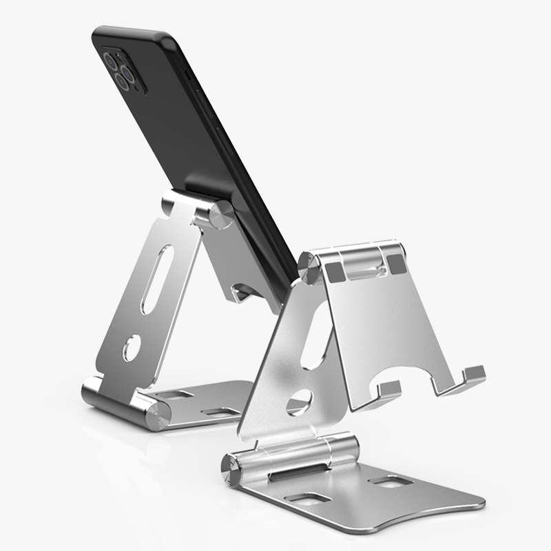
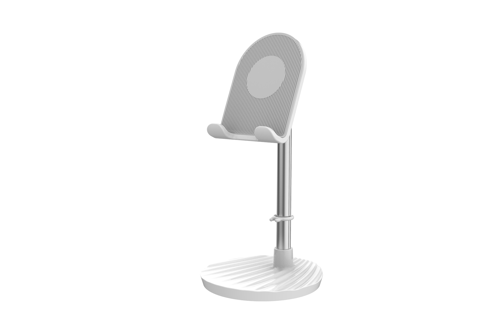
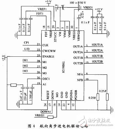
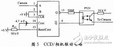
Compared with satellite and manned aerial aircraft remote sensing platforms, drones are characterized by low cost and high flexibility. In order to meet scientific remote sensing experiments, complete remote sensing tasks, coordinate multi-component work in drone electronic pods, and control the attitude of remote sensing image sensors, the system uses AT89S52 as the main control chip to extend the multi-channel serial port and USB interface to realize the system and peripheral devices. The communication is designed with the camera drive module and the three-degree-of-freedom stepper motor drive module. The UAV aerial remote sensing experiment proves that the system can meet the requirements of remote sensing experiments. USB interface expansion circuit design The USB port expansion is implemented by the CH375 chip. CH375 is a universal interface chip for the USB bus produced by Nanjing Yuheng Co., Ltd. Its main features are cheap price, convenient interface and high reliability. Support USB-HOST host mode and USB-DEVICE/SLAVE device mode. The USB host mode of the CH375 supports commonly used USB full-speed devices. The external MCU needs to write a firmware program to communicate with the USB device according to the corresponding USB protocol. However, for commonly used USB storage devices, the built-in firmware of the CH375 can automatically handle the dedicated communication protocol of Mass-Storage mass storage devices. Under normal circumstances, external microcontrollers do not need to write firmware programs. It is possible to directly read and write data in a USB storage device. There are two ways to communicate between CH375 and MCU: parallel mode and serial mode. The schematic diagram of the USB expansion circuit is shown in Figure 3. The CH375 chip is set to the built-in firmware mode using a 12 MHz crystal. The P0 port of the MCU is connected to D0~D7 of CH375 as the data bus, and the decoder output Stepper motor drive circuit The stable pan/tilt control is a three-degree-of-freedom stepper motor control, that is, controlling the pitch angle, the roll angle and the heading angle of the remote sensing sensor to maintain the stable pan/tilt in a horizontal (or vertical) state. The stepper motor drive is realized by the THB6128 chip. The single-chip microcomputer only needs to output the stepping motor running direction and pulse signal to achieve the purpose of controlling the stepping motor. THB6128 is a high-subdivision two-phase hybrid stepping motor driver dedicated chip. By outputting control signals through a single-chip microcomputer, a high-performance, multi-subdivided drive circuit can be designed. It features dual full-bridge MOSFET drive, low on-resistance Ron=0.55 Ω, maximum withstand voltage of 36 V, high current of 2.2 A (peak), multiple subdivision options, up to 128 subdivisions, with Automatic semi-flow locking function, fast decay, slow decay, hybrid attenuation, 3 attenuation modes, built-in temperature protection and overcurrent protection. Figure 4 shows the stepping motor drive circuit of the heading angle. The pitch angle and roll angle stepper motor drive are the same. In the figure, CP1 and U/D are respectively the driving pulse and motor running direction control signal given by the single chip microcomputer. M1, M2, and M3 are motor drive subdivision number selection signal inputs, which are controlled by the dial switch. FDT1 and VREG1 select the voltage and current control voltage inputs for the attenuation mode, respectively. When it is 3.5 V, it is slow decay mode; when it is mixed attenuation mode; when FDT1 is 0.8 V, it is fast decay mode. Adjust the VREG1 terminal voltage to set the stepper motor drive current value. CCD/camera drive circuit design The CCD/camera drive is implemented by a monostable flip-flop 74LS221 and an optocoupler P521. The 74LS221 can be either a falling edge trigger or a rising edge trigger, and both can disable the output. The pulse width of the output is obtained by internal compensation without external voltage and stability. In most applications, the pulse width is determined only by external timing components. The CCD/camera drive circuit is shown in Figure 5. The one-shot of the illustrated parameter has a high-level duration of approximately 33 ms. The charge time constant RC of the circuit can be changed to adjust the length of the steady-state time according to the actual exposure time of the camera. In the figure, Camera is the P3.5 port of the single-chip microcomputer. When it is the falling edge, it triggers the one-shot trigger output high level. This high level acts on the diode terminal of the optocoupler P521, thereby triggering the triode end conduction. Trigger the camera shutter. The output of P521 is connected in series with a 10kΩ resistor to prevent the current from being too large and causing damage to the camera. The data storage module is realized by AT24C512. The MCU P3.0 and P3.1 ports are respectively connected with the SCL and SDL ports of AT24C512, and the pull-up resistors are connected, and the I2C bus is extended to 64 KB E2PROM data memory. The SRAM extension is implemented by the IDT6116SA chip, which extends 2 KB to cache temporary data during microcontroller calculations. The system input voltage is 12 V DC, and the power module uses a series of 7805 and 7805 three-terminal regulators to reduce the voltage drop across the monolithic regulator and obtain a smooth +5 V voltage. | The experiment proves that the system can better meet the requirements of the airborne operation control of the UAV airborne remote sensing platform, coordinate the work of each component of the electronic pod, control the attitude of the camera, and downlink the onboard operation data in real time. There are fewer O ports, and the expansion of the USB interface solves the problem that many notebook computers do not have a COM port at present, and can process the photo information data in the operating system in time in the field experiment. The MCU still has more resources to use, which can facilitate the system upgrade, but it is also limited by the microprocessor data processing capability. 1. Desktop Mobile Phone Holder; open the Phone Holder directly to 45 degrees, put the phone on it and you can use it
5. Ring buckle mobile phone holder, the usage method only needs to stick the suction ring on the back of the phone, and then put the ring out to place the phone.
Phone Holder,Cell Phone Holder,Cell Phone Holder Bed,Cell Phone Holder Desk Shenzhen ChengRong Technology Co.,Ltd. , https://www.laptopstandsupplier.com![]() With CH375
With CH375 ![]() The chip is connected to the chip, and the MCU A0 is connected to the A0 of the CH375, and the address or data input and output of the CH375 can be selected. When A0 is high, the transmission of D0~D7 is the address, and when it is low, the data is transmitted. P3.6 and P3.7 control the read and write operations of CH375. CH375
The chip is connected to the chip, and the MCU A0 is connected to the A0 of the CH375, and the address or data input and output of the CH375 can be selected. When A0 is high, the transmission of D0~D7 is the address, and when it is low, the data is transmitted. P3.6 and P3.7 control the read and write operations of CH375. CH375 ![]() Single chip
Single chip ![]() At the input end, when there is data input through the USB port, an interrupt signal is generated to notify the microcontroller to perform data processing. After the CH375 chip is initialized and successfully connected to the host, the indicator light is on.
At the input end, when there is data input through the USB port, an interrupt signal is generated to notify the microcontroller to perform data processing. After the CH375 chip is initialized and successfully connected to the host, the indicator light is on. 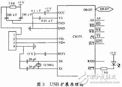
2. The bedside mobile phone holder; fix the clip of the mobile phone holder on the side of the bed, freely adjust the bending degree of the holder and the position of the mobile phone according to your posture, which is convenient and more comfortable.
3. Stick to the wall mobile phone bracket; the bracket sticker has strong adhesiveness and can be fixed and hung on glass, ceramic tiles and painted walls.
4. Car phone holder; car air outlet bracket, fixing method: After the mobile phone is installed on the mobile phone bracket, pop out the steel piece in the middle of the mobile phone bracket and put it into the car air outlet to fix it
