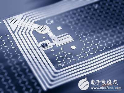
Radio frequency identification technology (RFID, Radio Frequency IdenTIficaTIon) is a recognition technology based on radar technology. The article discusses how to develop the RFID reader radio frequency circuit related information, including zero-IF demodulation technology, carrier circuit, signal modulation circuit and RF power amplifier circuit, and gives a program of RF circuit module structure, which simplifies the traditional RF circuits and the promotion of radio frequency identification (RFID) technology are of great significance in many fields such as industrial automation and traffic control. Radio frequency identification technology (RFID, Radio Frequency IdenTIficaTIon) is an identification technology based on radar technology. Its main principle is to use wireless electromagnetic waves to conduct non-contact two-way data communication to obtain relevant data and achieve target recognition. RFID technology is microwave. The emerging products of cross-disciplinary knowledge, such as technology, cryptography, and wireless communication principles, cover areas such as highway toll management, railway logistics transportation control management, and industrial automation monitoring. RFID system can be divided into low frequency (under 135kHz), high frequency 8197; (13.56MHz), ultrahigh frequency 8197; (860-930MHz) and microwave 8197; (2.4GHz above) according to the working frequency band. RFID systems usually consist of electronic tags (radio tags), antennas, and readers. The card reader is generally composed of a radio frequency signal processing module, a baseband signal processing module, a control unit, and an interface module connected with an external device. The RF signal processing module mainly implements three major functions: first, it transmits RF electromagnetic waves with sufficient power through an antenna to excite and provide energy for the electronic tag; second, it modulates the transmission signal and then converts the modulated signal data into electromagnetic wave transmission. To the tag; third is to receive and demodulate the RF signal from the electronic tag. In order to process data flow to and from the transponder in two directions, the RF signal processing module has two different signal channels. The data transmitted to the electronic tag is branched by the transmitting circuit, and the data from the electronic tag passes through the receiving circuit. Branch processing. The main function of the control unit: communicate with the upper application software and execute the commands sent by the application software; control the communication process with the electronic tag; signal encoding and decoding. For some specific systems, there are the following additional functions: implementation of anti-collision algorithm; encryption and decryption of data to be transmitted between the electronic tag and the reader; and two-way authentication between the electronic tag and the reader. The power of the transmitter signal of the reader is far greater than the backscattered signal of the electronic tag, and it is the same frequency as the received signal, so that if a high-power reflected signal leaks to the receiving circuit, the parts of the receiving circuit will be saturated, resulting in reading the card. The receiver cannot demodulate the received signal. Therefore, the technical specifications of the RF signal processing module will directly affect the quality level of the RFID system. The RF signal processing module generally includes two major units: one is a baseband signal modulation transmission module circuit, which is composed of a phase-locked loop circuit, a mixer modulation circuit, a filter circuit, and a power amplifier circuit; and the second is a demodulation and reception processing of a radio frequency signal. The circuit consists of a differential amplifier circuit, a zero-IF demodulator circuit and a corresponding filter circuit. (I) Zero-IF signal receiving and processing circuit RF signal receiving and processing circuit can be super-heterodyne circuit and zero-IF receiving circuit and so on. Since the zero-IF detection receiver has the advantages of simple implementation and low cost, its technical advantages are as follows: the frequency conversion relationship is simple, the nonlinear transformation components are less; the use of intermediate frequency SAW filter can be avoided; the intermediate frequency amplifier is not required, and the circuit structure is more concise , More cost-effective. As mentioned before, the modulation of the signal emitted from the electronic tag is Amplitude Keying Modulation 8197 (ASK), and it is in the same frequency as the carrier of the transmitter signal, and a four-channel zero-IF demodulation circuit is used in the RFID system. The signals at the four detection points in the circuit contain the transmitter's transmit signal and the received signal scattered from the tag. After they are diode-mixed, they are filtered by a low-pass filter to remove the high-frequency components. Tag data information and reader antenna and tag distance (reflected in the phase difference between the send and receive signals), where A, C two points in the signal will be in phase difference π, B, D is the same; separate them After the differential amplifiers D1 and D2 are fed into the amplifier, two output signals are obtained. Their amplitudes reflect the data information of the tags and are 90° out of phase, ie they are orthogonal. The signal is then amplified by differential amplifiers D3 and D4, respectively, and then through the comparator circuit, the IQ signal at the TTL level is finally sent to the baseband circuit for processing. Since the I and Q signals are orthogonal and only relate to the distance between the reader's antenna and the tag (according to the basic knowledge of the electromagnetic wave, it appears as the phase difference between the transmitted and received signals), that is, when The tag is located in the area covered by electromagnetic waves emitted by the reader antenna. At each determined time, the two signals are not only uniquely determined, but more importantly, the orthogonality of their phases guarantees that the two signals cannot be synchronized at the same time. Zero, this ensures that the circuit effectively captures the scattered signal from the electronic tag. (B) Modulation Transmitter Module Circuit The modulation transmitter circuit consists of three parts: a carrier signal generation circuit, a signal modulation circuit, and a radio frequency power amplifier circuit. 1. Carrier generation circuit. Figure 4 shows a carrier generation circuit. PLL400-915A is a phase-locked loop frequency synthesizer. It has good narrow-band filter characteristics and good phase noise. At the same time, it also has high output frequency purity and controllable frequency output. The chip can be controlled by the MCU through a program. The frequency of the output signal can be changed between 902MHz~928MHz, and the stepping frequency is 200kHz. This feature can facilitate users to implement wide-spectrum frequency hopping and improve the system's anti-interference ability. The TCX0 in the circuit is a temperature-compensated crystal that provides a stable, low-phase-noise, 12.8MHz reference frequency for the synthesizer. The SF2049E connected to the local oscillator signal output is a band-pass filter to filter out the higher harmonics of the output carrier signal and reduce the system noise. 2. Signal modulation circuit. The modulation circuit is shown in Figure 5. According to the RFID protocol standard, the transmitted signal uses ASK modulation. The circuit uses a low-noise RF amplifier chip RF2361 as a pre-driver for the RF power amplifier. The RF2361 has low noise, high intercept points, and controlled amplification. By adjusting the control terminal voltage VPD, its gain can be quickly reduced from 20dB to 0dB, that is, it is switched between the off state and the operating state by voltage control to achieve ASK modulation, and it can achieve very deep modulation depth. In this way, the encoded signal reaches the control of VPD through the driving circuit and the non-gate chip TC7S00, so that the ASK modulation of the encoded signal to the carrier is realized by the amplification control of the carrier. 3. RF power amplifier circuit. The RF power amplifier is a main component of a wireless transmitter. In order to efficiently radiate the modulated signal through the antenna in the form of electromagnetic waves, the RF signal must obtain a sufficiently large RF output power, so the RF power amplifier must be used before the signal is sent to the antenna. To amplify, the main technical indicator of the RF power amplifier is output power and efficiency. The important indicators of RF power amplifiers are: (1) The collector efficiency ηc is the ratio of the output power pout to the power supply power pdc, that is, ηc = pout / pdc; (2) Power increase efficiency 8197; (PAE, Power Added Efficiency) is the ratio of the difference between the output power pout and the input power pin to the power supply power pdc. (3) RF power amplifier linearity index has third-order intermodulation intercept (IP3), 1dB compression point, harmonics, adjacent channel power ratio. The adjacent channel power ratio measures the degree of interference with the adjacent channel caused by the non-linearity of the amplifier. (4) Spurious output and noise. In a transmission system, the output power of the RF final stage power amplifier can range from milliwatts (portable mobile communication equipment) to as much as several kilowatts (radio broadcasting). In order to achieve high power output, the preamplifier circuit of the final power amplifier must have a sufficiently high excitation power level. According to operating frequency and output power requirements, FETs, RF power integrated circuits, etc. can be used as RF power amplifiers. This system uses Hitachi's power amplifier chip PF01411A to achieve this task, as shown in Figure 6. PF01411A has small linear distortion, low input power requirement (0dBm is sufficient), gain control range up to 90dB, efficiency up to 45%, and maximum output power up to 5W. The MCU can control the output gain through the voltage control terminal Vapc to achieve the control of the RF output power. Liquid Crystal Display For Home Appliances Liquid Crystal Display For Home Appliances,High Resolution Portable Lcd Display,Refrigerator Lcd Liquid Crystal Display,Response Fast Remote Lcd Monitor Dongguan Yijia Optoelectronics Co., Ltd. , https://www.everbestlcdlcms.com