ADC reference voltage circuit design
Overview:
The overall accuracy of a high resolution, successive approximation ADC depends on accuracy, stability, and drive capability of its reference. The switched capacitor at the ADC reference input has a dynamic load, so the reference circuit must be able to handle the current associated with the time and throughput rate. Some ADCs have an on-chip reference and a reference buffer on-chip, but these devices may not be optimal in terms of power or performance—typically using an external reference circuit for optimum performance. This article explores the challenges and requirements encountered in the design of voltage reference circuits.
A simplified schematic of the reference voltage input successive approximation ADC is shown in Figure 1. During the sampling interval, a capacitive DAC is connected to the ADC input and a charge proportional to the input voltage is stored in the capacitor. After the conversion starts, the DAC is disconnected from the input. The conversion algorithm switches each bit one by one to the reference voltage or ground. The redistribution of charge on the capacitor can cause current to flow into or out of the reference voltage source. The dynamic current load is a function of the internal clock of the ADC throughput rate and control bit verification. The most significant bit (MSB) holds most of the charge and requires most of the current. 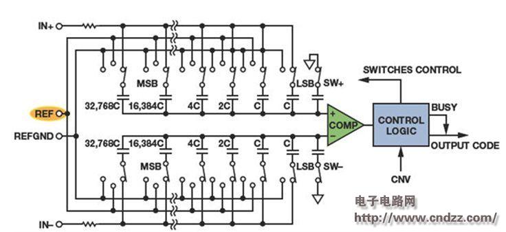
Figure 1. Simplified diagram of the 16-bit successive proximity ADC principle
Figure 2 shows the dynamic current load of the AD7980, 16-bit, 1 MSPS, PulSAR successive approximation ADC reference input. The measured value is obtained by observing the voltage drop across the 500 Ω resistor between the reference and the reference pin. The curve shows current spikes up to 2.5 mA with small spikes throughout the transition. 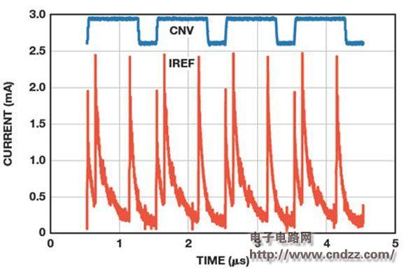
Figure 2. AD7980 Dynamic Reference Current To support this current while maintaining the noise-free characteristics of the reference, place a high-value, low-ESR storage capacitor as close as possible to the reference input, typically 10 μF or greater. Larger capacitors further smooth the current load and reduce the burden on the reference circuit, but extremely large capacitance can cause stability problems. The reference must be able to supply the average current required to fill the reference capacitor without causing the reference voltage to drop too much. In the ADC data sheet, the average of the reference input current is typically specified at a specific throughput rate. For example, in the AD7980 data sheet, the average reference current for a 5 V reference at 1 MSPS is specified as 330 μA typical. No current is consumed between conversions, so the reference current varies linearly with throughput rate and drops to 33 μA at 100 kSPS. The reference – or reference buffer – must have a sufficiently low output impedance at the highest target frequency to maintain a voltage level at the input of the ADC so that the voltage does not cause too much voltage drop due to current.
(Please read the PDF for details)
Withstand high voltage up to 750V (IEC/EN standard)
UL 94V-2 or UL 94V-0 flame retardant housing
Anti-falling screws
Optional wire protection
1~12 poles, dividable as requested
Maximum wiring capacity of 6 mm2
T06 Series Terminal Blocks,Wire Connectors Terminal Block,Wire Connector For Led,Wire Connector Assortment
Jiangmen Krealux Electrical Appliances Co.,Ltd. , https://www.krealux-online.com